1.Research Background
Similar to the development path of traditional microelectronic chips, the emergence of photonic quantum chips is an inevitable trend in advancing photonic quantum information technology toward practical applications. Currently, mainstream photonic quantum chips mainly rely on probabilistic photon sources based on nonlinear optical processes to generate single-photon signals. However, due to the probabilistic nature of photon emission, these sources suffer from low emission efficiency and difficulties in preparing multi-photon qubits.
In contrast, solid-state emitters (such as self-assembled quantum dots and diamond color centers) possess atom-like two-level energy structures that enable deterministic and highly efficient single-photon emission. They are thus ideal light sources for realizing on-chip preparation of multi-photon qubits. Nevertheless, solid-state quantum light sources still face major challenges such as inhomogeneous spectral broadening and the lack of efficient heterogeneous integration techniques. These issues severely limit their applications in large-scale on-chip integration and quantum network interconnection, becoming a key bottleneck in the practical development of photonic quantum chips.
To address these challenges, Prof. Jiaxiang Zhang and Dr. Xin Ou from the Shanghai Institute of Microsystem and Information Technology, Chinese Academy of Sciences, together with Prof. Jin Liu from Sun Yat-sen University and Prof. Yongheng Huo from the University of Science and Technology of China, have published a new study in Nature Materials entitled “Large-scale quantum-dot–lithium-niobate hybrid integrated photonic circuits enabling on-chip quantum networking.” In this work, the team innovatively realized a hybrid integrated photonic quantum chip that combines deterministic single-photon sources based on semiconductor quantum dots with low-loss thin-film lithium niobate. They proposed an on-chip local stress tuning technique based on ferroelectric domain engineering of lithium niobate thin films, achieving broadband, highly dynamic, and reversible spectral fine-tuning of quantum-dot single-photon sources.
Moreover, the researchers developed a “micro-transfer printing” heterogeneous integration process with sub-100-nanometer precision, enabling the simultaneous on-chip integration and spectral tuning of up to 20 deterministic quantum-dot single-photon sources. Through innovations in material functionality and hybrid chip architecture, the team demonstrated on-chip quantum interference and interconnection between spatially separated quantum-dot single-photon sources for the first time on a hybrid integrated photonic quantum chip—laying an important foundation for building scalable on-chip quantum networks.
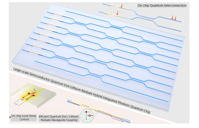
Large-scale Semiconductor Quantum Dot–Lithium Niobate Hybrid Integrated Photonic Quantum Chip
2.Research Highlights
(1) By combining two quantum materials with outstanding advantages in optical research—self-assembled quantum dots and lithium niobate—the team addressed the long-standing challenge of scalable multi-photon state generation in photonic quantum chips. They developed an innovative “micro-transfer printing” hybrid chip integration process, achieving the hybrid integration of 20 deterministic quantum-dot single-photon sources with a low-loss lithium niobate photonic chip. This work establishes the largest-scale hybrid integrated photonic quantum chip based on deterministic quantum-dot sources reported internationally to date.
(2) To overcome the intrinsic inhomogeneous broadening problem of on-chip solid-state quantum systems (such as quantum dots and diamond color centers), the researchers proposed a novel DC voltage-driven local stress control technique based on ferroelectric domain engineering of lithium niobate thin films. This approach integrates five key features :on-chip integration, broadband tunability, 4 K cryogenic compatibility, ultra-low power consumption (on the order of mW), and reversible tuning. Beyond expanding the functional capabilities of lithium niobate beyond traditional electro-optic modulation and surface acoustic wave control, this technique opens a new dimension of on-chip quantum control, and provides technical guidance for applying other emerging ferroelectric thin-film materials such as barium titanate (BTO) and strontium titanate (STO) in quantum control applications.
3.Key Breakthroughs
1.A novel mechanism for stress regulation on lithium niobate thin films was proposed, enabling on-chip dynamic stress tuning of deterministic quantum-dot single-photon sources. The achieved spectral tuning range of 7.7 meV exceeds the transform-limited linewidth of quantum-dot single photons by three orders of magnitude.
2.A hybrid integration process with sub-100-nm precision was developed, enabling simultaneous on-chip integration and spectral tuning of up to 20 deterministic quantum-dot single-photon sources. Based on this platform, the team realized on-chip quantum interference interconnection between different quantum-dot single-photon sources, achieving an on-chip interconnection distance of 0.48 mm and an interference visibility of 73%.
3.The on-chip stress control technique based on lithium niobate ferroelectric domain engineering demonstrates compatibility with 4 K cryogenic operation, temperature-insensitive stress output, high spatial locality, and ultra-low power consumption. These advantages make it possible to simultaneously integrate thousands of quantum-dot light sources on a single chip, providing an important technological pathway for scalable on-chip multi-photon resource generation.
4.Figure Interpretation
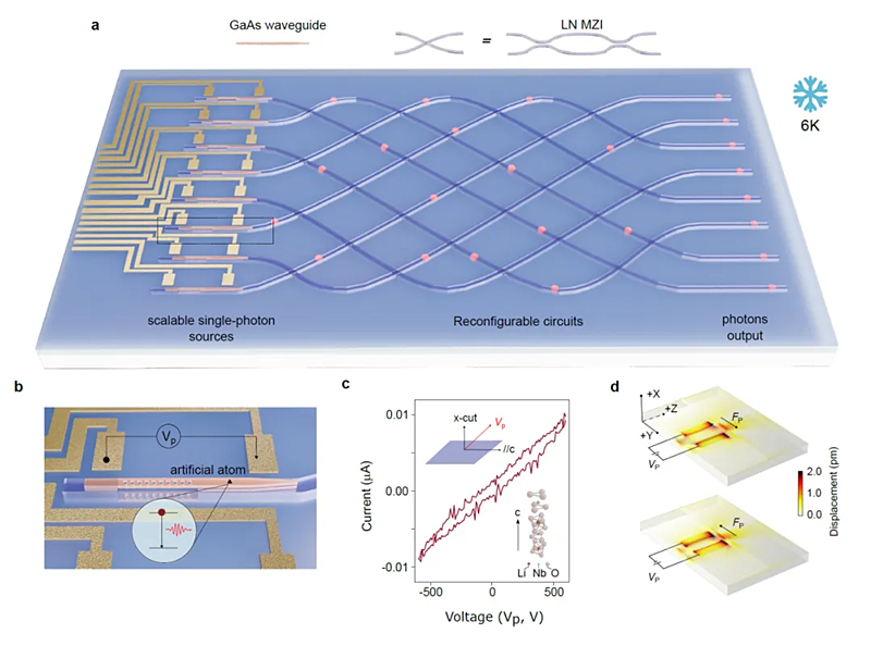
Figure 1:
(a) Large-scale semiconductor quantum dot–lithium niobate thin-film hybrid integrated photonic quantum chip.
(b) Hybrid quantum dot–lithium niobate integrated waveguide with local stress control functionality.
(c) On-chip local stress generation achieved at cryogenic temperature via DC-driven ferroelectric domain engineering on X-cut lithium niobate thin films.
(d) Anisotropic local stress distribution on the lithium niobate thin film.
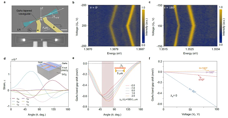
Figure 2:
(a) GaAs quantum dot–lithium niobate hybrid integrated waveguides with different orientations; the single-photon signals can be extracted either through the waveguide top or via a grating coupler.
(b, c) On-chip stress tuning for waveguides of different orientations.
(d) Numerical simulation of the orientation-dependent stress tensor distribution.
(e, f) Numerical simulations of the orientation-dependent band structure tuning of quantum dots.
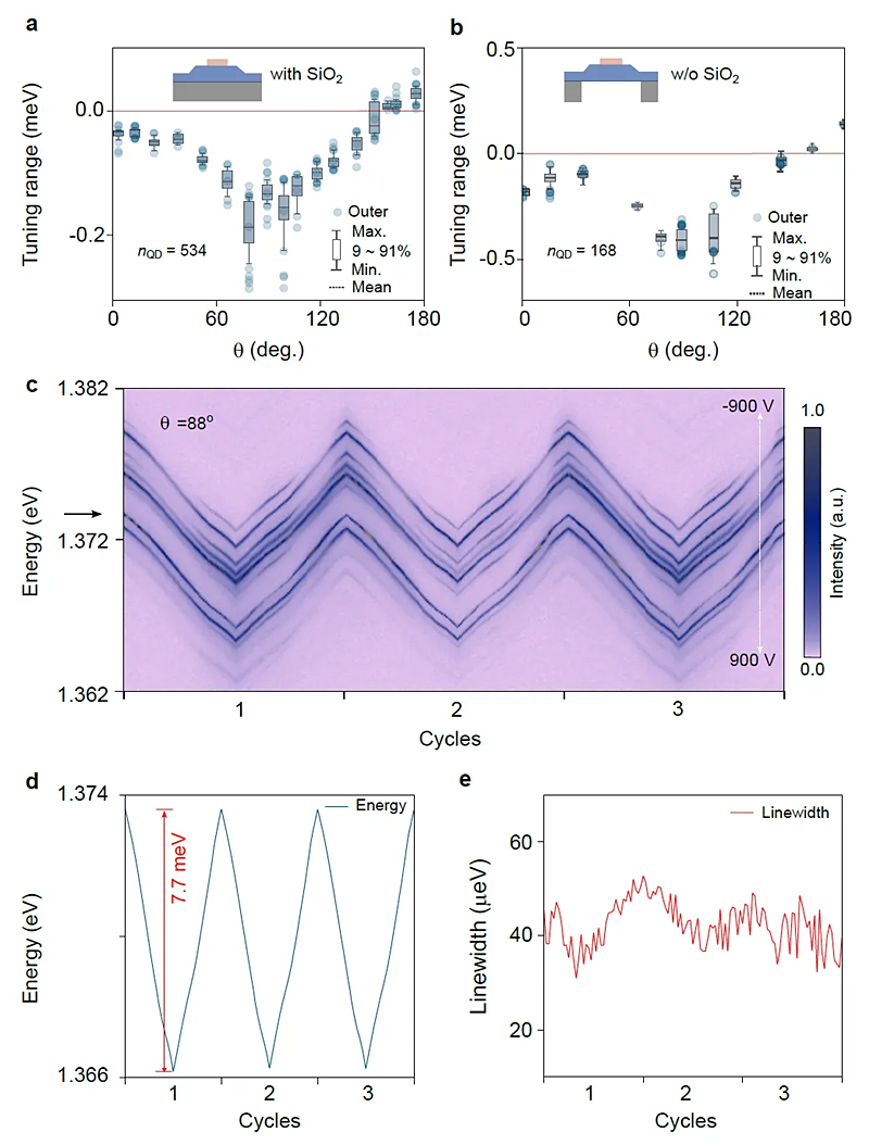
Figure 3:
Statistics of orientation-dependent local stress tuning ranges of quantum dots.
(a) Quantum dot–lithium niobate hybrid waveguide with a SiO₂ insulating support layer.
(b) Quantum dot–lithium niobate hybrid waveguide without a SiO₂ insulating layer.
(c) Reversible and broadband spectral tuning of waveguide-coupled quantum dots at the optimized orientation angle (88°),
(d) showing a tuning range of 7.7 meV.
(e) Variation in single-photon emission linewidth during local stress tuning of quantum dots.
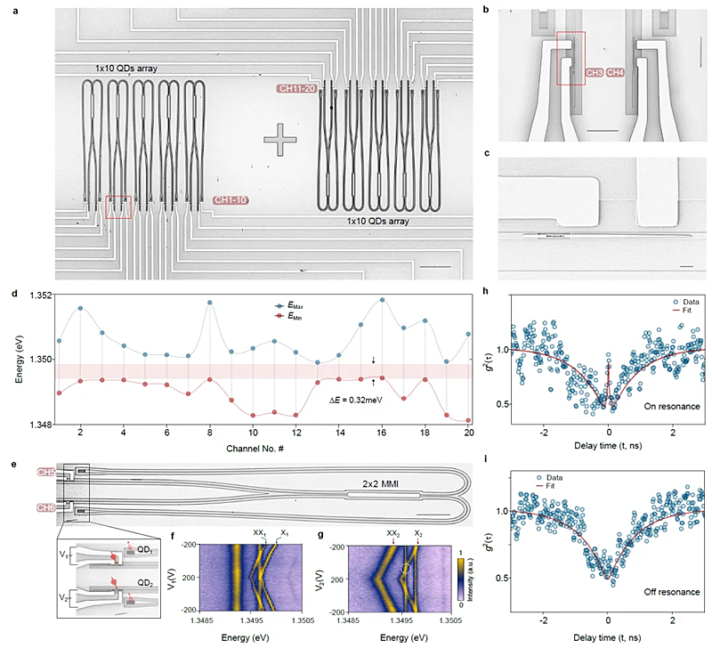
Figure 4:
(a) Lithium niobate hybrid integrated photonic quantum chip incorporating 20-channel deterministic quantum-dot single-photon sources.
(b, c) SEM images of the quantum dot–lithium niobate hybrid integrated waveguides.
(d) Simultaneous local spectral tuning of 20 on-chip deterministic quantum-dot single-photon sources; local tuning range: 0.76 meV/400 V. The red region indicates the “frequency-matched” region after tuning of the 20 channels.
(e, f, g) Simultaneous local tuning of two spectrally distinct quantum dots located in channels 5 and 6.
(h, i) Two-photon resonance measurements of the two waveguide-coupled quantum dots on the chip.
5.Future Outlook
This work combines two quantum materials with significant advantages in optical research—self-assembled quantum dots and lithium niobate—providing a new technological route for the scalable development of photonic quantum chips. The platform also exhibits strong scalability potential: the current on-chip integration density of quantum-dot single-photon sources reaches 67 per mm, meaning that a centimeter-scale chip could accommodate over 1,000 quantum channels.Moreover, the local stress control of a single-channel quantum-dot single-photon source requires only microwatt-level power consumption, which is three orders of magnitude lower than the milliwatt-level thermo-optic tuning typically used in silicon photonic chips. Its low-temperature compatibility and ultra-low power operation also make it feasible to integrate superconducting nanowire single-photon detectors (SNSPDs) on the same chip.The research team further notes that in the future, the high-speed electro-optic effect of lithium niobate can be exploited to realize on-chip high-speed photon routing and entanglement distribution, offering a novel technological pathway toward fault-tolerant linear optical quantum computing and a scalable quantum internet.
The first author of the paper is Dr. Xudong Wang from the Shanghai Institute of Microsystem and Information Technology (SIMIT).The corresponding authors are Prof. Yongheng Huo (University of Science and Technology of China), Prof. Jin Liu (Sun Yat-sen University), and Dr. Xin Ou and Dr. Jiaxiang Zhang (SIMIT).This research was supported by the National Key Research and Development Program of China (2022YFA1404604), the CAS Youth Innovation Promotion Association (YSBR-112), and the National Natural Science Foundation of China.
