
How far known-good-die screening reaches — and what happens to the part it cannot reach, What a wafer probe covers, what it cannot, how statistics bridge the gap, and what KGD actually delivers.
Put a bare die into a module, test it, and find it fails — by then the most expensive part is already attached. That was the pluggable-era approach, and the cost was tolerable. In the co-packaged era it is not, so screening has to happen before the wafer is diced.
That is where known-good die (KGD) comes from. What it actually screens, and how far it reaches, is rarely spelled out. This article draws the boundary.
1. Why it has to happen before dicing
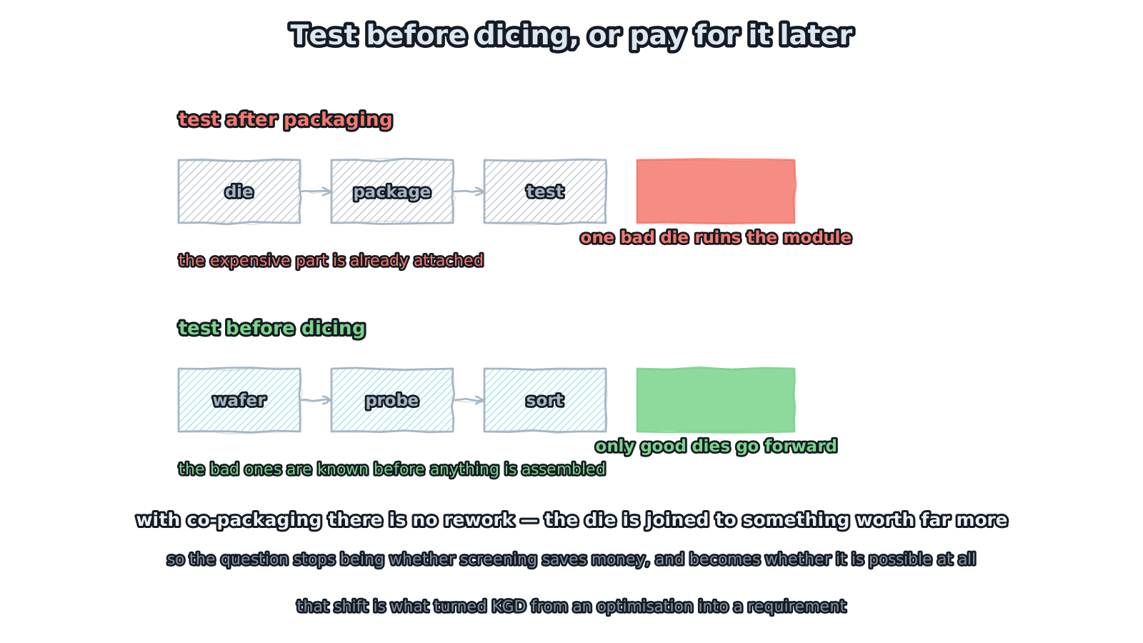
Figure 1 — Test before dicing, or pay for it later
with co-packaging there is no rework — the die joins something worth far more
Start with the difference between the two flows.
The traditional one is test after packaging: the die comes in, gets packaged into a module, and is then tested. If it fails, the whole module is scrap — and the most expensive thing in that module is not the die. It is the package, the fibre attached to it, the driver electronics inside.
The other route is test before packaging: the wafer goes on a prober, every die is measured, failures are marked in place, and after dicing only the confirmed good ones move forward.
In the pluggable era the first route was affordable — modules are self-contained, and one bad unit is one swap. With co-packaging, the optics share a substrate with the switch die and there is no rework: one bad die destroys an assembly worth far more than itself. So the question stops being whether screening pays for itself and becomes whether it is possible to skip it.
That shift is the whole reason KGD moved from optimisation to requirement.
2. What the probe reaches
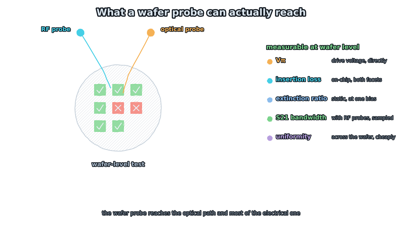
Figure 2 — What a wafer probe can actually reach
Vπ, on-chip loss, static extinction ratio, sampled bandwidth, uniformity
A wafer prober does more than most people assume. Optically, probes couple light into the waveguide from above and collect it again; electrically, RF probes land on the electrodes and measure the response. So these parameters are available before dicing.
Drive voltage, Vπ — sweep the bias through the transfer curve and read the half-wave voltage straight off. This is the central figure and the easiest to measure accurately at wafer level.
On-chip insertion loss — couple in and out through probes and what you measure is exactly the number that appears on the datasheet.
Static extinction ratio — the peak-to-null ratio of that same transfer curve.
RF bandwidth — S21 with an RF probe, though usually sampled rather than measured on every die, because high-frequency prober time is expensive.
Uniformity across the wafer — the largest bonus of wafer-level test. Several hundred dies in minutes gives you the distribution, and process drift becomes visible immediately. That is something post-package testing can never do.
3. What it genuinely cannot reach
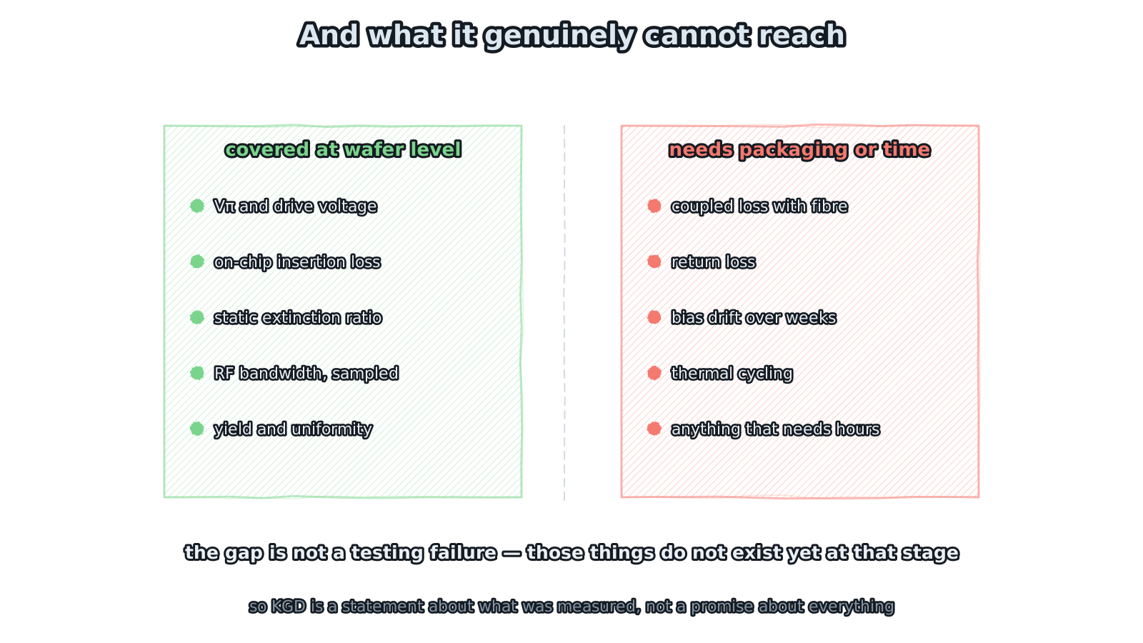
Figure 3 — And what it genuinely cannot reach
the items needing packaging or time do not exist yet at that stage
Some items are not merely hard to measure. They do not exist yet at that stage.
Coupled loss as built — probe coupling and final fibre coupling are different things. Mode, alignment, gel, stress: all of it happens after packaging. Those 3.3 dB from the previous article can only be inferred indirectly at wafer stage.
Return loss — likewise needs a real fibre interface to exist.
Bias drift over time — the subject of an earlier article. It unfolds over weeks and months; a prober cannot wait.
Thermal cycling — needs a package, a chamber, and hours.
Listing these is not a criticism. It is the point: KGD is a statement about what was measured, not a promise that everything is fine. When buying it, knowing what was not covered matters as much as knowing what was.
4. Bridging the gap
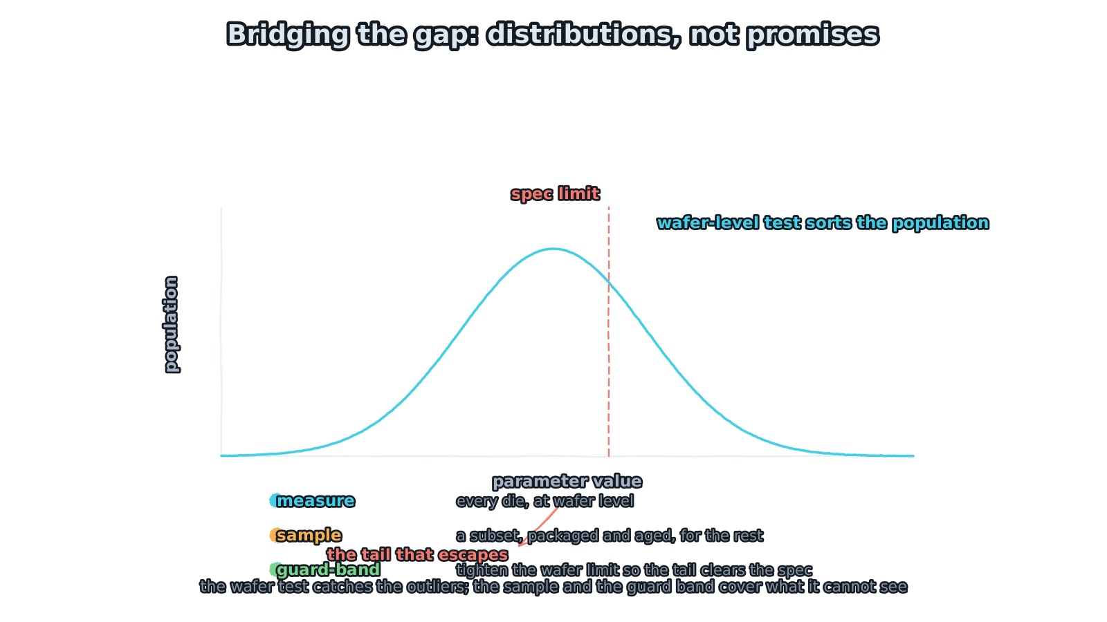
Figure 4 — Bridging the gap: distributions, not promises
measure every die, sample the rest, and guard-band the tail out
Since part of the picture cannot be measured directly, the risk has to be pushed down another way. Three techniques, used together.
The first is measure everything: run every die through whatever can be measured. That removes the obvious outliers, and it is the most effective single step, because most failures are discrete and show up as a clear parameter excursion.
The second is sampling: take a subset from the same lot, package it, and run the full test programme including everything that needs time. The behaviour of that subset stands in for the lot. How much you sample and how you choose it determine how strong that inference is.
The third is guard-banding: tighten the wafer-stage criteria so the tail of the final distribution falls outside the specification. The cost is yield — tighten one notch and you discard parts that would probably have passed. It is an explicit trade: yield for confidence.
Only the three together constitute a guarantee. A KGD programme that does just the first has done half the job.
5. What actually gets delivered
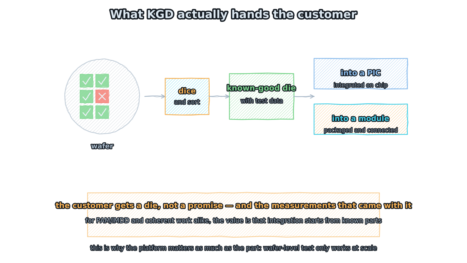
Figure 5 — What KGD actually hands the customer
a die and its measurements — not a promise
Finally, what lands on the receiving dock. It is a bare die plus the measurements that came with it — not a packaged module, and not an assurance that it will work.
That form is genuinely useful downstream. Customers building an integrated photonic circuit need bare dies, because the modulator goes onto the same chip as everything else. Customers building a module need bare dies because they have their own packaging flow and their own alignment scheme. What both share is that integration starts from known parts rather than unknown ones — true for PAM/IMDD and coherent work alike.
One more thing worth saying. Wafer-level test only makes sense on a platform running at scale. A prober, a set of criteria, a statistical process — all of it needs volume to amortise. That is why the platform matters as much as the part: being able to test at wafer level is itself evidence that a process line has reached a certain maturity.
6. What to ask
If KGD is what you need, these are the items worth pinning down.
Which parameters were measured — ask for the list, not a blanket "everything". What the criteria are — the pass window for each one. Which are sampled — the ratio and the method. How the unmeasurable part is handled — accelerated ageing data, guard bands, and how much margin was left. How the data arrives — a measured value per die, or just a pass mark; the former lets the customer run a second screening pass. Lot-to-lot consistency — whether the distribution holds across lots.
That last one is the easiest to skip and the most telling. One good lot does not mean the next will match. What has real value is a distribution that is stable — that says the process is under control, not that this batch got lucky.
Closing
KGD sounds like a promise. It is really a list: what was measured, against what criteria, what was not, and what covers the rest.
Read it as a list and you can use it properly. It lifts the starting point of integration from unknown to known, which is worth a great deal. It does not replace post-packaging verification, and it does not replace time.
Known-good die lets integration begin from the known. As for what only time can tell, it merely moves the waiting somewhere cheaper.
* Figures are hand-drawn vector schematics illustrating structure and principle; they do not represent the actual shape, dimensions or layout of any specific product.
* Test items, criteria and statistical methods described are illustrative of common industry practice; specific programmes depend on process platform, product type and customer requirements.