
Open a modulator datasheet and the insertion loss reads 3.5 dB. Put the die in a module, measure again, and it says 6.8 dB. Same chip. Where did the extra three decibels go?
All of it sits at the two facets. This article opens up that bill: where the loss goes, why thin-film devices are harder to couple to than most, and the three fixes the industry reaches for.
1. The same chip, two numbers
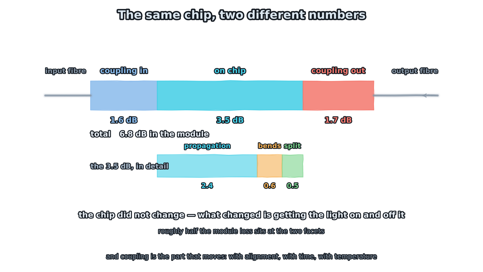
Figure 1 — The same chip, two different numbers
the chip did not change — getting light on and off it did
Lay the whole chain out flat. From input fibre to output fibre, the loss splits three ways.
The middle is the chip itself: waveguide propagation, bend loss, and the intrinsic cost of splitters or combiners — 3.5 dB in total. That is set by material and layout, and once the wafer is out it cannot be changed.
The two ends are coupling: light into the chip and back out again, 1.6 and 1.7 dB. That is 3.3 dB, very nearly as much as the entire chip.
So "3.5 on chip, 6.8 in the package" translates to this: packaging costs about as much loss as the chip does. Which is why coupling is never an incidental detail — it is half of module design, on equal footing with the die.
One more thing that tends to be overlooked. The 3.5 dB on chip is fixed. The 3.3 dB at the facets moves — with alignment, with time, with temperature. Whatever drifts in a reliability test is almost always this term.
2. Mode mismatch
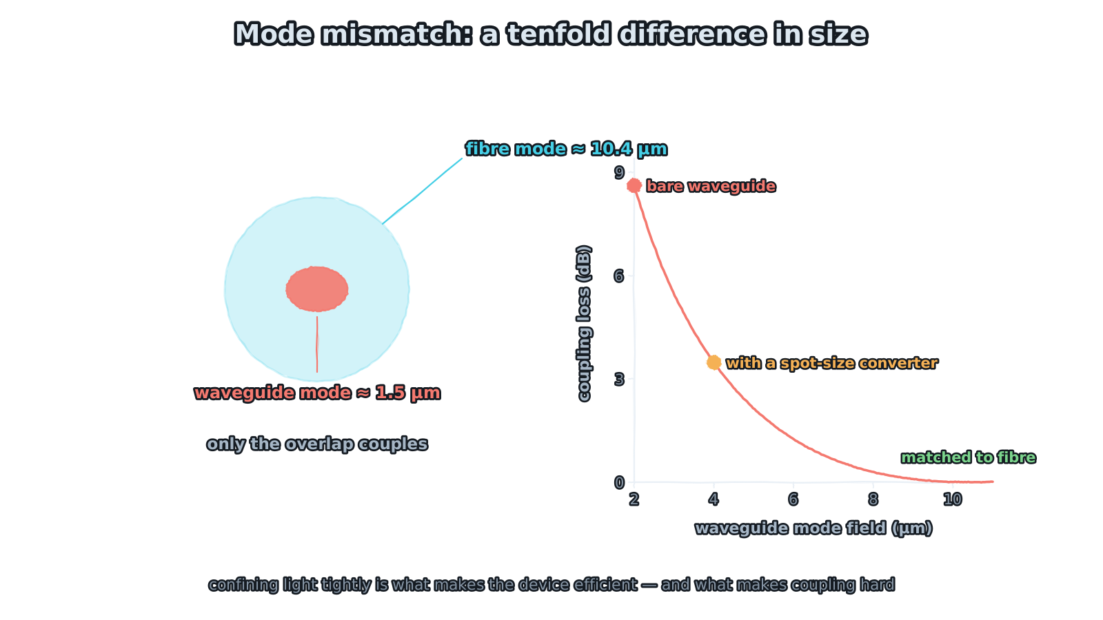
Figure 2 — Mode mismatch: a tenfold difference in size
the tighter the confinement, the harder the coupling — two faces of one thing
The single largest contributor to coupling loss is that the two mode fields do not match.
Single-mode fibre at 1550 nm has a mode field diameter of about 10.4 µm. A thin-film lithium niobate waveguide, confining light tightly, comes in around 1.5 µm — a factor of nearly ten. Coupling between two Gaussian modes follows their overlap integral, and at an order-of-magnitude size difference the mismatch loss is in the region of 10 dB. That is not "some loss"; that is unusable.
There is a trade-off here that cannot be designed around, and it is worth stating plainly. Tight confinement is exactly what gives a thin-film device its low drive voltage: a small mode lets the electrodes sit close, and Vπ·L follows it down. But the same geometric change pushes the mode away from anything a fibre can deliver. Low voltage and small mode are two faces of one thing, and the small mode is what makes coupling hard.
Which means a thin-film platform can never be coupled bare. The mode has to be expanded first — the first of the three fixes below.
3. How tight the tolerance is
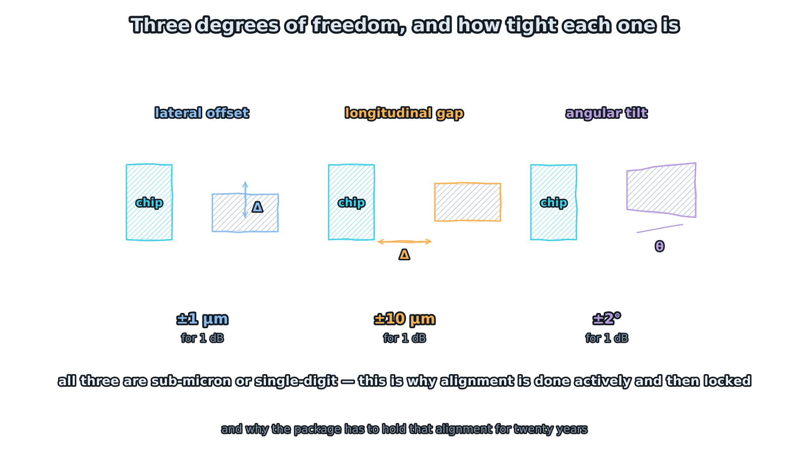
Figure 3 — Three degrees of freedom, and how tight each one is
sub-micron laterally, a couple of degrees in tilt — align actively, then lock
Even with the modes matched, alignment is a fight. A fibre has six degrees of freedom relative to the chip; three of them do most of the damage.
Lateral offset is the most sensitive — tolerance for 1 dB is sub-micron, roughly ±1 µm. Fibres sit on a 250 µm pitch, and you have to place one to within a micron: the equivalent of locating a few millimetres across several hundred metres.
Longitudinal gap is far more forgiving, around ±10 µm, because the beam diverges only modestly over ten microns. Once index-matching gel is in place the beam no longer diverges in air at all, and this term nearly disappears.
Angular tilt comes in at roughly ±2°. It is sensitive because the distance from facet to mode is short, so a small angle throws the spot off centre quickly.
Three axes, all sub-micron or single-digit. That is why fibre attach has to be active alignment — light running, six axes trimmed to the power maximum, then laser-welded or bonded in place. It is also why long-term package stability matters so much: that micron has to still be there in twenty years.
4. Reflection comes back at you
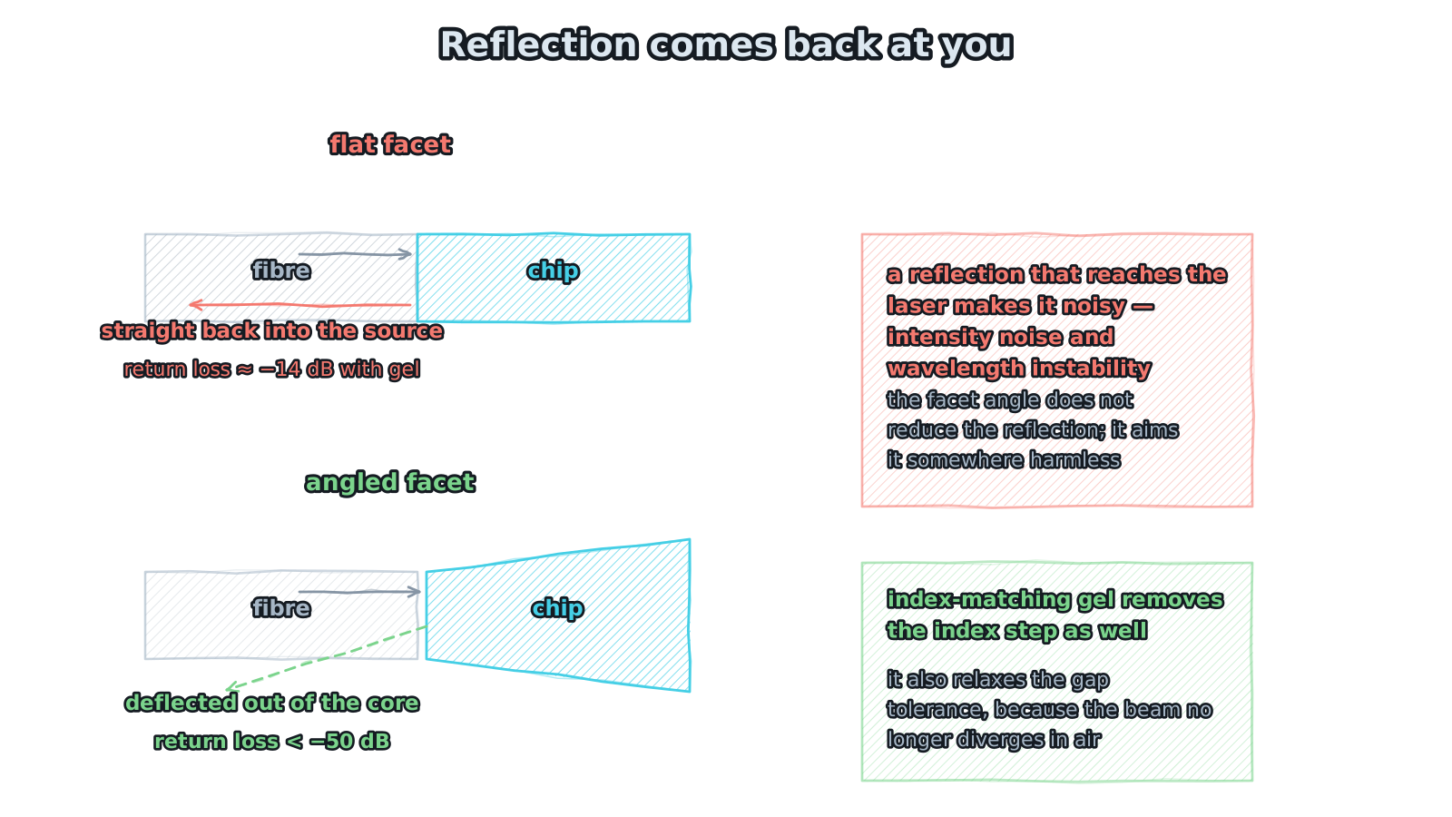
Figure 4 — Reflection comes back at you
the angle does not reduce reflection; it aims it somewhere harmless
There is one more term that has nothing to do with power but matters just as much: return loss.
Light crossing from fibre into chip meets a refractive index step — roughly 1.45 in silica to about 2.2 in lithium niobate. Fresnel reflection is unavoidable, and a flat facet with no gel returns only about −8 dB. That light travels straight back and arrives at the laser.
The consequence is a worse laser: relative intensity noise rises, wavelength stability suffers, and narrow-linewidth applications are hit hardest. Return loss is not a hygiene metric; it acts directly on the source.
Index-matching gel improves this to around −14 dB, which is still not enough. The real fix is an angled facet, typically 8°. One common misunderstanding is worth clearing up: the angle does not reduce the reflection — it aims it into the cladding and the housing instead of back down the core. The reflection is still there; it just lands somewhere harmless. Angled facet with gel reaches better than −50 dB.
5. Three ways to win it back
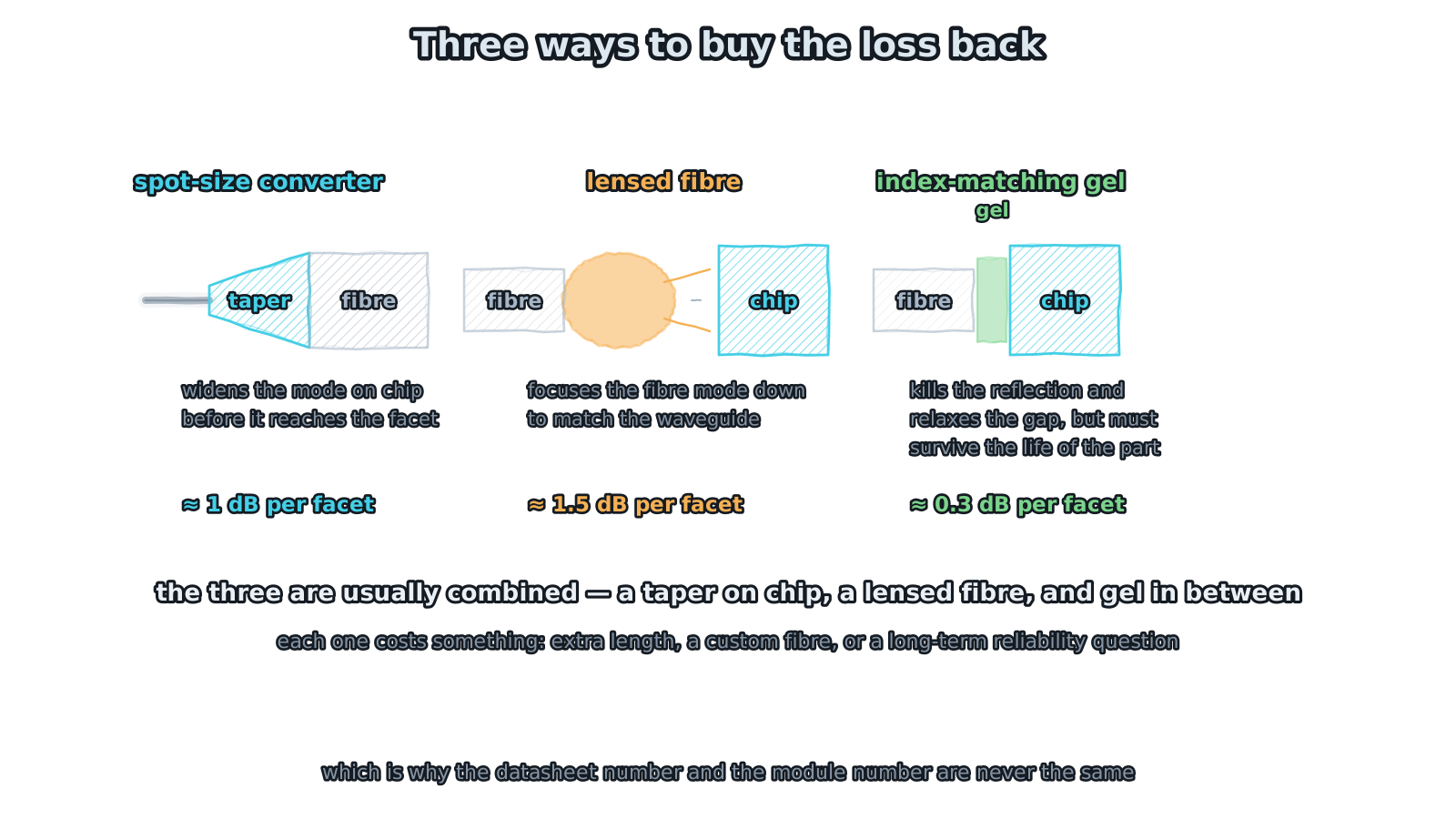
Figure 5 — Three ways to buy the loss back
usually all three at once, and each costs something
Back to the question: how are those decibels recovered? Three main approaches, usually combined.
The first is a spot-size converter: taper the waveguide near the facet so the mode expands before it leaves the chip, from 1.5 µm out to three or four microns or more. At 4 µm the mismatch loss drops from the 10 dB region to around 3.5 dB. The cost is extra chip length and an extra process step.
The second is a lensed fibre: shape the fibre tip into a lens or taper so the 10.4 µm mode is focused down to a few microns to meet the chip. Around 1.5 dB per facet, at the cost of a custom fibre that still needs precision alignment.
The third is index-matching gel between the facets, removing the index step. On its own it recovers only about 0.3 dB, but it also fixes return loss and relaxes the gap tolerance, which makes it close to mandatory.
Stacked together, one to 1.5 dB per facet is achievable in volume. Each comes with a price, though: extra die length, a custom fibre, and a gel joint that has to survive the life of the product. Which is why on-chip loss and module loss are never the same number — you cannot have the first without paying for the second.
6. What to ask on delivery
Pulling it together, these are the items worth pinning down when reading a specification or writing one.
Is the loss on-chip or in-module — ask first; the gap is the coupling. Does it include both facets — some quote one. What is the return loss — insertion loss alone is not enough, and poor return loss drags the laser down. Polarisation-dependent loss — coupling is polarisation sensitive, and a large PDL shows up as extra fluctuation in a real system. Drift after temperature cycling — coupling is the one term that moves with time and temperature, so ask for the change across cycling, not the initial value. Which approach — is there a spot-size converter, a lensed fibre, and what is the gel and its lifetime data.
That last one is often skipped, and it is what determines long-term behaviour. Coupling is not finished at assembly. It is a sub-micron condition that has to hold for the life of the part.
Closing
Back to the opening question. The difference between 3.5 dB and 6.8 dB sits entirely at the two facets, and it comes from a piece of physics that is awkward to avoid: confining light tightly is what makes the device good, and confining it tightly is what makes coupling hard.
Coupling loss is therefore not an incidental packaging overhead. It is one of the central engineering problems of a thin-film photonics platform, and deserves the same attention as modulation efficiency or bandwidth. Three techniques help; each has a cost; usually all three get used.
When you read a datasheet, ask where the insertion loss was measured from and to. The few dB in between are exactly what engineers have spent twenty years aligning.