
Over the past few years the photonics industry has quietly changed the question it keeps asking. Ten years ago everyone wanted to know how far a single fibre could carry a signal. Today the question is how many picojoules a bit costs. Every time AI training clusters double in size, the bandwidth demanded by intra- and inter-rack interconnect climbs with them — while the power budget barely moves. The power density of pluggable optical modules is closing in on the thermal limits of the chassis, and the equalisation penalty paid by electrical signals travelling a dozen centimetres across a PCB is eating the gains that each bandwidth upgrade was supposed to deliver.
So attention has swung back to the devices themselves. Is there an electro-optic material that keeps the clean, strictly linear electro-optic effect of lithium niobate, yet — like silicon photonics — lets you shrink the device, pull the electrodes close together and bring the drive voltage down? Thin-film lithium niobate (TFLN) is the answer that has emerged, and it is the most substantial engineering breakthrough in photonic integration of the past decade. This article walks a complete optical link end to end — modulators, sources, detectors, and on to nonlinear frequency conversion — to lay out what this device stack can genuinely do today, and where it is still constrained.
1. Squeezing the light: three payoffs from going thin
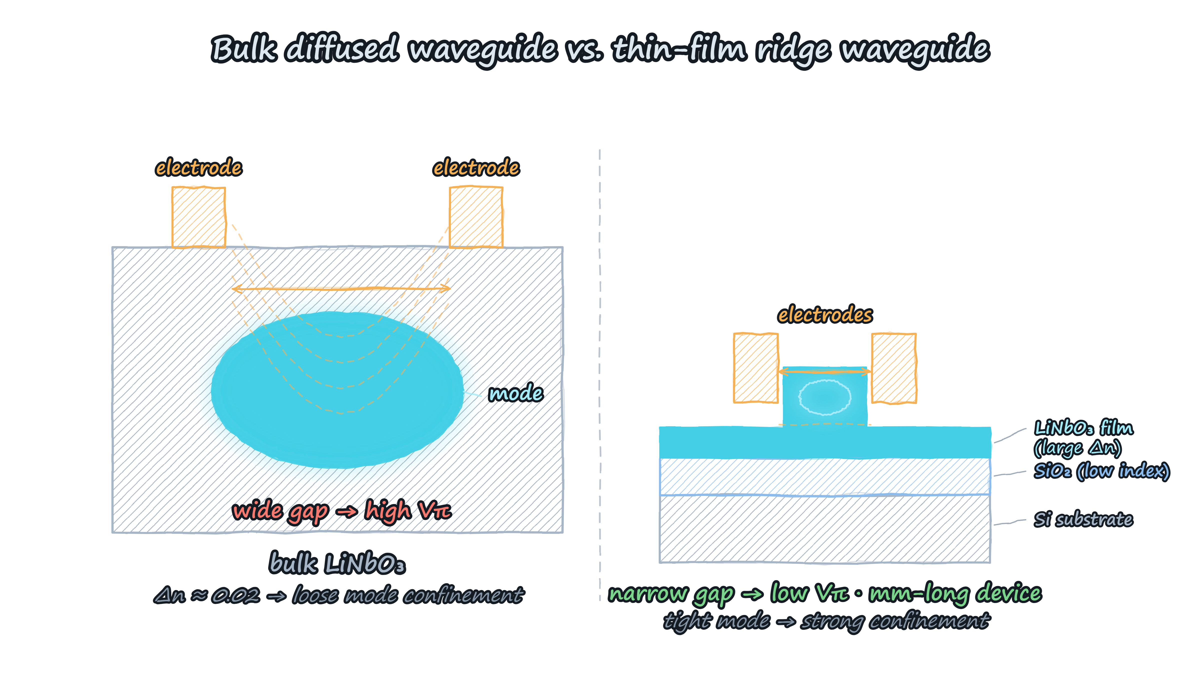
Figure 1 — Bulk diffused waveguide vs. thin-film ridge waveguide: tighter optical confinement, and a narrower electrode gap that follows from it
Mode area shrinks by one to two orders of magnitude — half-wave voltage, device length and drive power all improve together
Conventional bulk lithium niobate modulators build their waveguides by titanium indiffusion or proton exchange. The problem with that approach is not poor performance — quite the opposite. Its loss is extremely low, it handles high optical power, and its long-term stability is excellent, which is why it still carries the majority of long-haul coherent traffic. The problem is that the index contrast is simply too small, typically on the order of 0.02. A small index step means the optical mode cannot be held tightly: the mode field diameter is often around ten microns, and a large fraction of the optical energy wanders deep into the bulk of the material.
Once the mode is that large, a chain reaction follows.
The electrodes have to sit far apart. The electric field has to cover the whole mode, so the electrode gap must match the mode size — usually ten microns or more. A wide gap means more voltage for the same amount of phase modulation, so the half-wave voltage Vπ stays high; commercial bulk devices commonly sit at 4–6 V.
Velocity matching gets hard. The microwave effective index and the optical group index differ substantially, so the travelling-wave electrodes need elaborate slow-wave design to pull the two into alignment, and device lengths run to several centimetres.
Drive power resists compression. High voltage × long electrodes = a large capacitive load, and driver dissipation becomes a system-level burden — especially at 1.6T, where every port needs its own driver.
Thin-film technology turns this whole set of physical relationships inside out. Thin the lithium niobate crystal down to sub-micron thickness and bond it onto a silicon dioxide cladding — silica sits at roughly 1.44, far below lithium niobate’s ~2.2, so the upper and lower claddings create a very large index step and the light is pinned inside a film a few hundred nanometres thick. Etch a ridge into it, and the mode area can be one to two orders of magnitude smaller than in the bulk case.
This pays off three ways, and the three reinforce each other: the electrode gap can drop to a few microns or less, field strength rises as the inverse of the gap, and the half-wave voltage–length product Vπ·L falls accordingly; device length collapses from centimetres to millimetres, which simultaneously eases both microwave loss and velocity mismatch in the travelling-wave electrodes; and the small mode also means nonlinear interaction strength climbs steeply, which sets up the frequency conversion discussed further down.
To be clear, thin film is not unconditionally better than bulk. The mode of a thin-film waveguide is badly mismatched to standard single-mode fibre, and edge-coupling loss remains one of the most painful parts of volume production. Etched sidewall roughness introduces scattering loss. And lithium niobate’s intrinsic photorefractive effect and DC drift deserve more attention, not less, at small dimensions and high optical power density. None of these are questions of principle — they are questions of yield and cost, and they are where today’s process platforms actually differ.
2. Modulators: how much you can do with one interferometer
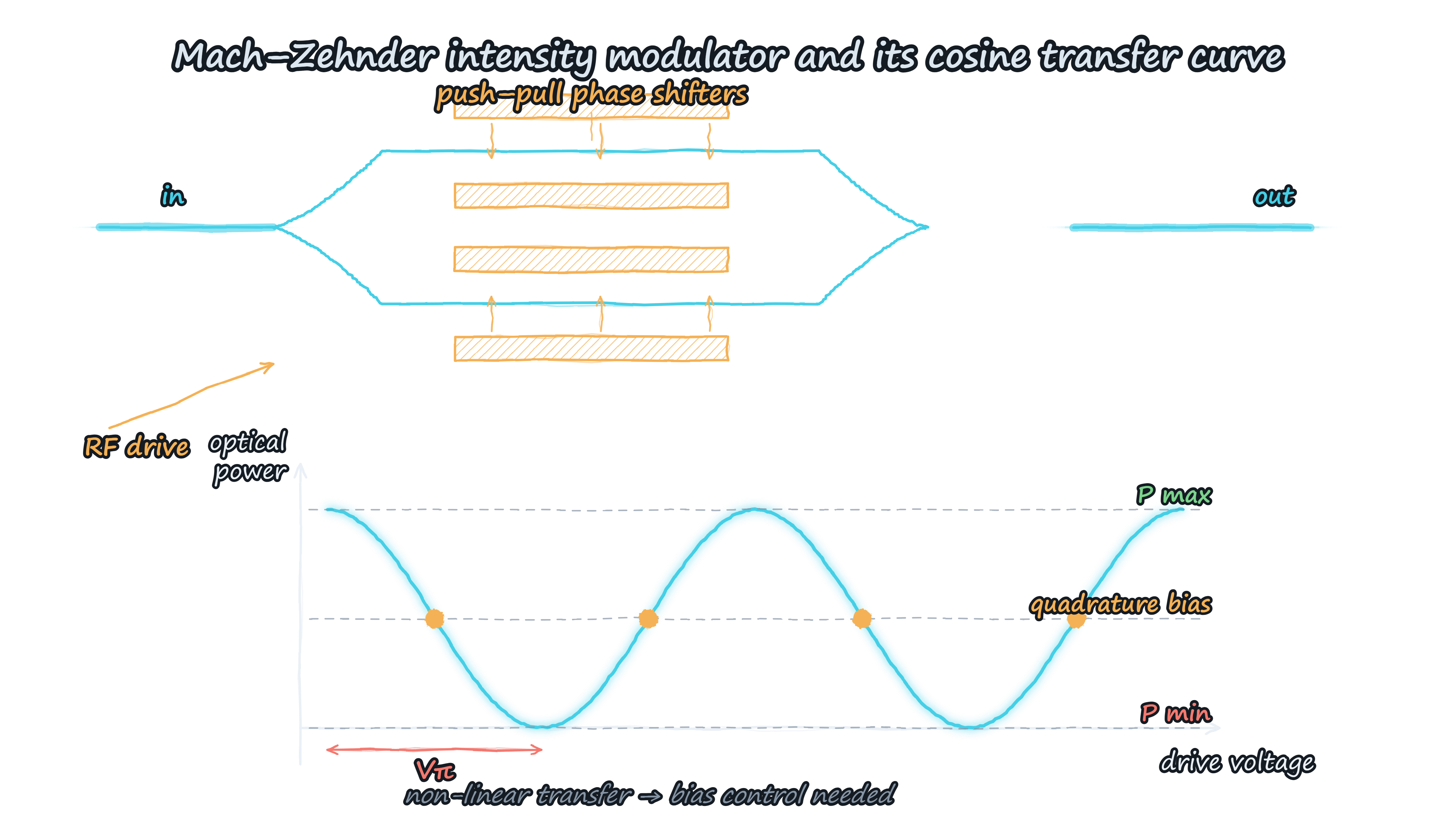
Figure 2 — Mach–Zehnder intensity modulator: push–pull electrode structure and the cosine transfer curve
The static operating point is normally locked at quadrature, with bias control circuitry fighting DC drift
Almost every lithium niobate intensity modulator is built on a Mach–Zehnder interferometer (MZI). The incoming light is split in two, each half passes through an arm modulated by the electric field, and the two recombine and interfere. With a push–pull phase difference applied across the arms, output power varies cosinusoidally with voltage — which is exactly why the transfer curve is non-linear, and why bias-point control is unavoidable in practice.
Quadrature bias is the default choice: park the static operating point where the slope of the transfer curve is steepest. Output power is then about half the peak, modulation linearity is best, and second-harmonic distortion is at its lowest. But DC drift in lithium niobate makes that point wander slowly, so real modules always carry a bias control loop — either detecting a low-frequency dither at the output (the pilot-tone method) or monitoring optical power directly — to lock the operating point back. This is the step that people evaluating modulators most often overlook: a pretty small-signal S21 plot does not mean the module will hold the same extinction ratio after hours of operation.
Beyond intensity modulators, the same platform generally also supports phase modulators, and monolithic hybrid integration of a DFB laser with an intensity modulator. The latter is attractive for IMDD (intensity modulation / direct detection): it removes the coupling interface between laser and modulator, saving 1–2 dB of link budget straight away and eliminating one potential failure point.
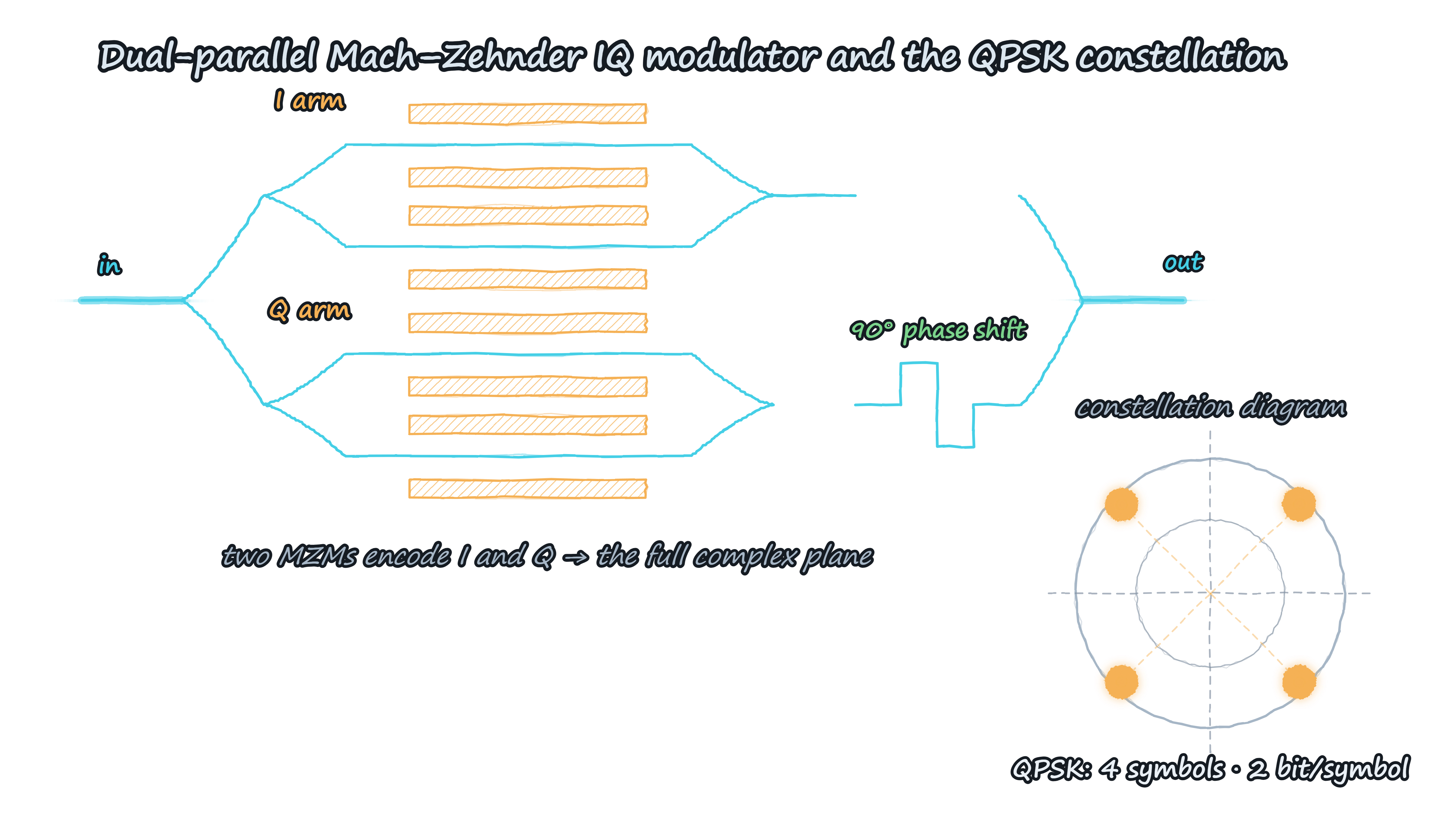
Figure 3 — Nested dual-parallel Mach–Zehnder IQ modulator and the QPSK constellation
Two MZMs encode I and Q respectively; one path receives an extra 90° optical phase shift
The next step up is the IQ modulator, also known as the dual-parallel Mach–Zehnder (DP-MZM). Structurally it is two MZMs in parallel, each branch encoding the in-phase and quadrature components respectively, with one path adding a 90° optical phase shift. Recombined, the two branches can place symbols anywhere in the complex plane — which is the physical basis for higher-order formats such as QPSK and 16QAM. Today’s production capability sits at roughly 60 GBd symbol rate, supporting RF mixing and single-sideband modulation up to 60 GHz, enough to cover the great majority of coherent and RF-over-fibre requirements.
Here is a design detail that is routinely underestimated: high-end IQ modulators use a folded-optics layout that puts the RF interface and the optical interface at opposite ends of the device. That is not cosmetic. If RF feed lines and the fibre array are crowded onto the same side, packaging and routing fight each other and high-frequency signal integrity is hard to guarantee. Physically separating the two is what keeps impedance continuity intact at the RF port — and above 60 GHz that is close to decisive.
3. The source fork: direct modulation, or external?

Figure 4 — Two transmitter architectures: direct modulation + direct detection (top) vs. external modulation + coherent detection (bottom)
The former trades reach for cost; the latter trades complexity for capacity
This fork largely determines the cost structure and the reach ceiling of the whole link, which makes it worth pulling out on its own.
The directly modulated laser (DML) route modulates the injection current of a DFB laser so that output power follows the current. The structure is simple, the cost is low and the power draw is small, which makes it the undisputed workhorse of short-reach data-centre interconnect. Off-the-shelf parts routinely deliver 3 dB bandwidth above 30 GHz, enough for 100G per lane and beyond with PAM4. The standard package is a 7-pin butterfly with an RF (K) connector, an integrated thermoelectric cooler, an optional isolator, and a polarisation-maintaining fibre pigtail terminated in FC/APC connectors. Wavelengths cover the O band (1310 nm) and C band (1550 nm), with extension to the L band available.
But the DML has a physical ceiling it cannot get around. Direct modulation changes the carrier concentration, which changes the refractive index of the active region at the same time, so the instantaneous optical frequency jitters along with the intensity: that is chirp. Chirp combined with fibre chromatic dispersion broadens the pulse as it propagates, and the penalty grows with distance. This is also why the 1310 nm window is so hospitable to DMLs — the dispersion coefficient of standard single-mode fibre passes through zero near 1310 nm, so the chirp penalty is suppressed for free. On top of that, the bandwidth ceiling of direct modulation is set by the relaxation oscillation frequency; pushing further means very high injection current density, and both stability and lifetime have to be compromised accordingly.
External modulation separates “making light” from “modulating light” completely. The laser only has to deliver continuous-wave output with stable power and a very narrow linewidth; the modulation is handed to a separate electro-optic modulator downstream. The cost is one more component, one more coupling interface and one more slice of power. The return is that chirp is essentially zero, the modulation format can be changed at will, and phase becomes something you can manipulate — and only on this path does coherent communication become possible at all.
So the selection logic is actually quite clear. For intra-rack interconnect from a few hundred metres to roughly ten kilometres, PAM4 + DML + direct detection is unbeatable on cost and power. For metro, long haul, and any scenario that needs higher-order modulation to fight dispersion, external modulation with coherent reception is the only answer. The genuinely interesting ground is in between: hybrid integration of a DFB laser with a thin-film lithium niobate modulator on a single platform, trying to approach DML-like cost with external-modulation signal quality. That is one of the directions most worth watching right now.
4. At the receiver: the three-way trade-off behind 110 GHz
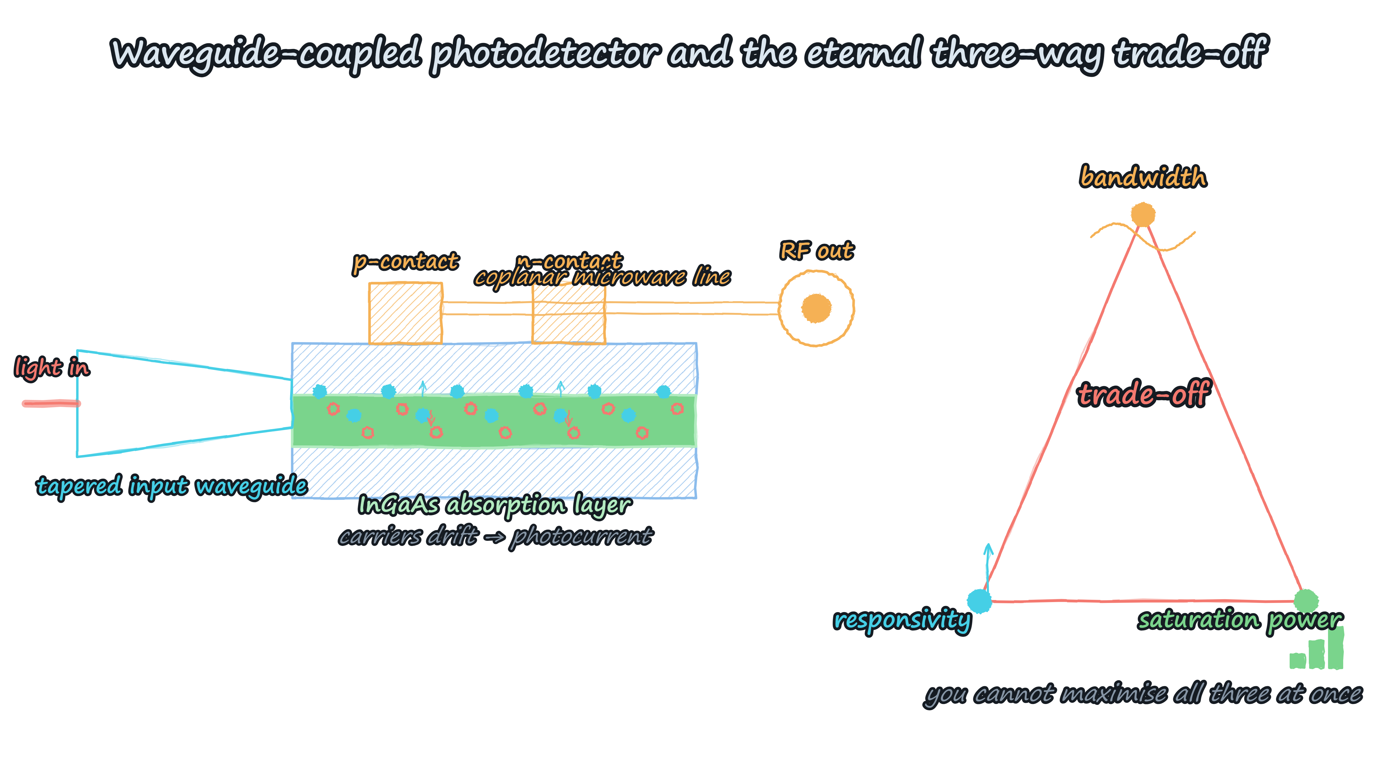
Figure 5 — Cross-section of a waveguide-coupled photodetector, and the bandwidth / responsivity / saturation-power trade-off triangle
The waveguide (edge-coupled) geometry decouples the absorption direction from the carrier transit direction
With the transmitter done, the optical signal eventually has to become current again. Indium phosphide has almost no serious competitor in this position: it integrates the absorption layer, the waveguide structure and the high-speed junction on a single epitaxial stack, reaching 3 dB bandwidths on the order of 110 GHz while keeping dark current and reliability acceptable. An InGaAs absorption layer natively covers the short-wave infrared from 780 to 2500 nm, which conveniently takes in both the datacom O band (1310 nm) and the telecom C band (1550 nm).
Photodetector design, however, is never a contest for a single headline number. It is a tug-of-war between three parameters:
Bandwidth vs. responsivity. A thinner absorption layer shortens carrier transit time and raises bandwidth — but light also travels a shorter distance, quantum efficiency drops, and responsivity falls with it. This is the most direct of the contradictions, and the waveguide geometry exists precisely to break it: let the light propagate laterally along the absorption layer so that the transit direction is decoupled from the absorption direction, and you can have high bandwidth and high responsivity at once.
Bandwidth vs. saturation power. Shrinking the junction area reduces junction capacitance and lifts the RC bandwidth ceiling, but optical power density then climbs steeply, and space-charge effects make the response saturate early at high power, bringing non-linear distortion with them.
Noise vs. gain. A PIN structure offers good linearity and high speed, but the signal needs amplification downstream. An APD brings internal gain and higher sensitivity, at the price of excess noise, temperature sensitivity and a much higher bias voltage. Only in very weak-light scenarios — quantum and sensing — do APDs and single-photon detectors come into their own.
Coherent reception adds one more specific requirement: balanced detection. Two closely matched detectors receive the two outputs of the local-oscillator/signal mixing, and the difference is taken, cancelling the local oscillator’s relative intensity noise and driving up common-mode rejection. That places very real process demands on how well the two diodes are matched — which is why photodetectors for coherent receivers usually ship as screened pairs.
5. Changing the wavelength: periodically poled lithium niobate and quasi-phase-matching
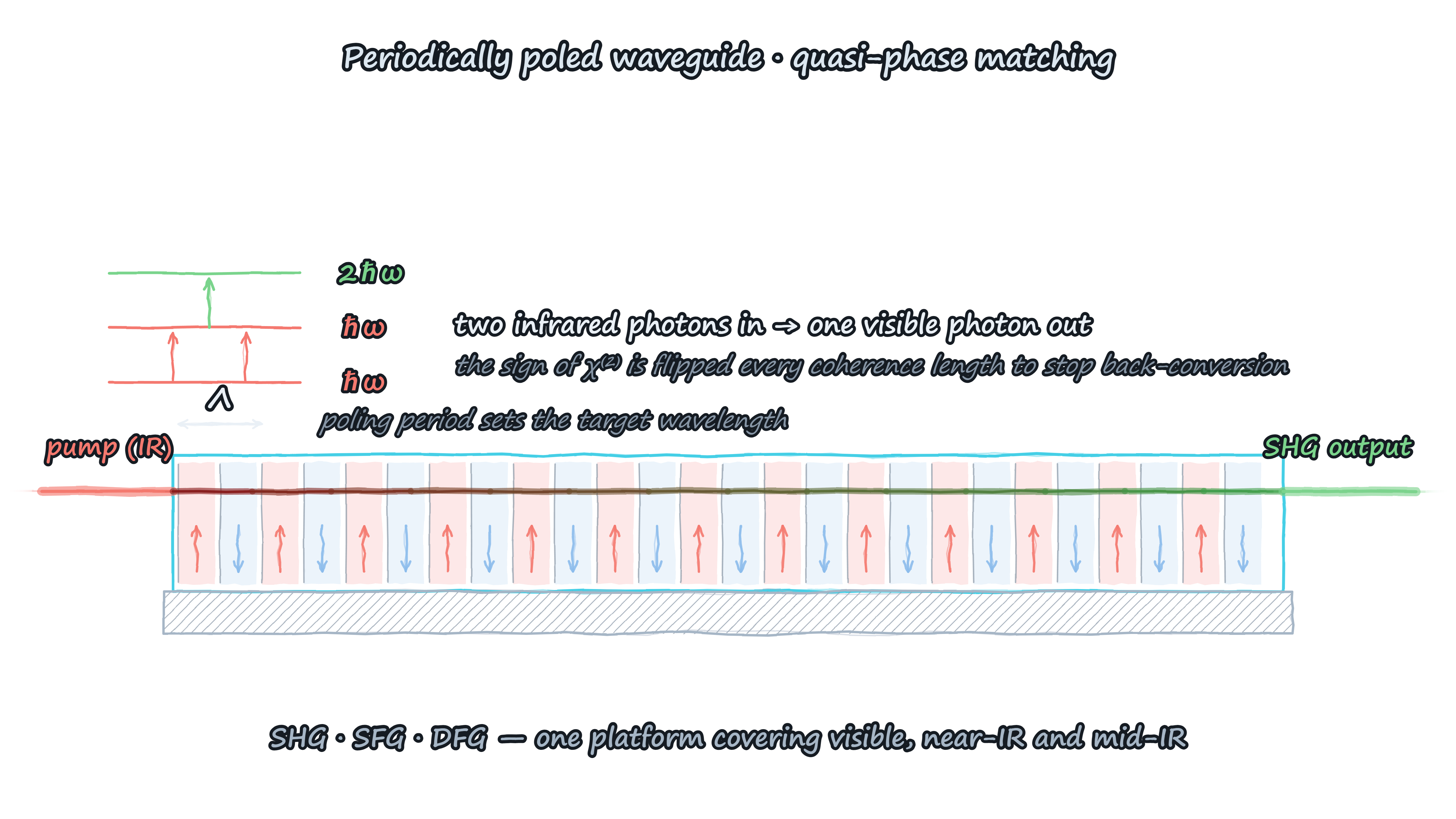
Figure 6 — Quasi-phase-matching in a periodically poled waveguide: domain inversion compensates the phase mismatch
An infrared pump is converted progressively to visible along the waveguide; the period Λ sets the target wavelength
The first four sections have all been about using light to carry information. But lithium niobate holds another card: it is also an excellent second-order nonlinear material, able to change the colour of light outright.
The trouble with second-order nonlinear processes is phase matching. Light of different wavelengths travels at different speeds in the material, so the fundamental and the second harmonic fall out of step after some distance, energy sloshes back and forth between them, and net conversion efficiency goes nowhere. The traditional fix exploits birefringence, using the anisotropy of the crystal to line up the refractive indices of different polarisations — but that route is constrained by crystal orientation and often cannot reach the largest nonlinear coefficient.
Quasi-phase-matching (QPM) turns the problem around. If phase mismatch accumulates, then flip the sign of the nonlinear coefficient every half coherence length so that the back-converting energy is turned forward again. Physically, that means applying a high-voltage field to periodically pole the lithium niobate, producing a PPLN whose ferroelectric domains alternate with a period typically between a few and a few tens of microns. The benefit is immediate: the largest coefficient, d33, becomes usable, and conversion efficiency runs an order of magnitude above birefringent schemes. Better still, the period is designable — given a pump wavelength and a target wavelength, the required period follows — so visible, near-infrared and mid-infrared are all within reach.
In practice, PPLN modules are waveguide-based: confine the light to a cross-section of a few square microns over a few centimetres and the interaction strength rises more than two orders of magnitude above a bulk crystal, so watt-level pumping gives useful conversion efficiency. The module integrates a thermoelectric cooler and thermistor for temperature tuning, because temperature both fine-tunes the phase-matching condition and suppresses photorefractive damage. When ordering, specifying pump and target wavelengths (SHG, SFG or DFG) to two decimal places is what gets you the right poling period.
The application space is wider than many people assume. Spectroscopy needs narrow-linewidth sources tuned onto gas absorption lines; fluorescence microscopy needs picosecond and femtosecond sources at specific wavelengths; environmental monitoring and medical diagnostics are all moving this way. These are fields that used to depend on bulky solid-state lasers with external cavity doubling — waveguide PPLN has lowered that barrier considerably.
6. Moving a single photon: quantum frequency conversion

Figure 7 — Quantum frequency conversion: telecom-band single photons are shifted into the visible and handed to a silicon detector
The hard part is not conversion efficiency — it is avoiding even one spurious noise photon
This may be the most counter-intuitive section in the article. If fibre loss is lowest at 1550 nm, why would you ever move a photon away from that band?
The answer sits at the detector. Quantum communication and quantum networks want to transmit at 1550 nm, where fibre loss is only 0.2 dB/km. But the silicon single-photon detectors that are efficient, cheap and operate at room temperature perform best in the visible — particularly around 780 nm — and at 1550 nm you are forced back onto expensive, deeply cooled detectors. Hence the compromise: perform quantum frequency conversion at the end of the link, move the telecom-band single photon into the visible, and detect it with cheap silicon.
The difficulty is that this is conversion at the single-photon level. The process itself has to be clean: any surplus noise photon directly contaminates the quantum state, destroying entanglement and single-photon statistics. Second-harmonic generation from the strong pump, and spontaneous Raman scattering, both contribute background photons, so the module needs dedicated wavelength-separation design to filter these by-products out before they reach the detector. At the same time, conversion efficiency has to be high, or the fidelity of the qubit degrades even faster. Low background plus high conversion efficiency — those two metrics are usually harder to achieve, and far more discriminating between approaches, than raw power conversion efficiency.
Conversion modules targeting 780 nm and 532 nm output are already productised, serving long-distance quantum communication, quantum networking and quantum precision measurement. The market is nowhere near the size of the data centre, but the demands on device performance are in many dimensions more severe — a classic small-volume, high-barrier segment.
7. The form-factor debate: from pluggable to co-packaged
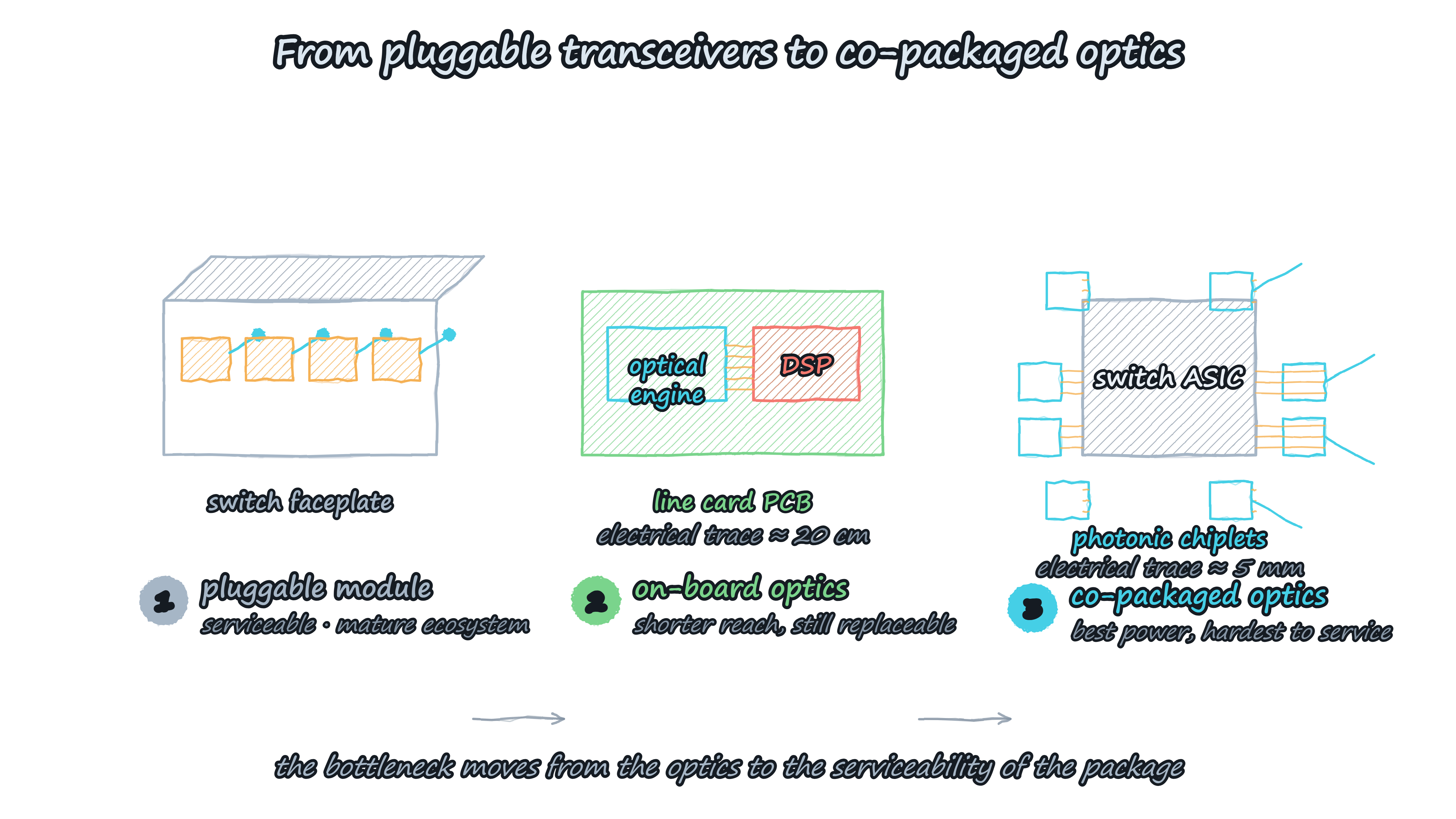
Figure 8 — Evolution of optical interconnect packaging: faceplate pluggable modules → on-board optical engine → co-packaged with the switch ASIC
The electrical interconnect shrinks from 20 cm to 5 mm, and the bottleneck moves from the devices to serviceability
Back to the system level. However good the devices are, they still have to answer the question of where they sit.
Pluggable modules remain the mainstream. They are operations-friendly, the ecosystem is mature, and a failed unit can simply be swapped. The industry already has coherent transceivers that densely integrate a broadband, compact thin-film LiNbO₃ modulator with a silicon photonics receiver inside a standard pluggable form factor. Exploiting the excellent transmission performance and low loss of the TF-LN modulator, those products deliver high output power and high OSNR, translating to roughly 15% more transmission distance than the previous generation. That sounds modest, but on long-haul routes it means real savings in site count and build cost. The next target is next-generation 1.6 Tbps pluggable coherent transceivers.
Further along sits co-packaged optics (CPO). The idea is to move the optical engine right next to the switch ASIC, replacing a dozen centimetres of PCB trace with a few millimetres of electrical interconnect, and removing the SerDes power and signal-integrity problem in one move. On this path, the low drive voltage of thin-film lithium niobate gets amplified in value: a lower drive voltage means a simpler, more efficient driver, and that is precisely the cost item CPO is most sensitive to.
What actually holds CPO back, though, is not device performance — it is the engineering ecosystem. How do fibres get attached at the faceplate at high density while remaining serviceable? How do optical chiplets get known-good-die (KGD) tested and screened at wafer level? How does thermal design accommodate temperature-sensitive optics sitting next to a very hot switch chip? And most practically: how are field replaceability and fault isolation procedures going to be redefined? Until those are solved, performance advantages of any size stay on paper.
Appendix: four device families, key capabilities and selection criteria

Figure 9 — Key capabilities, typical volume metrics and selection criteria for the four device families
Figures are typical values for volume and pre-volume parts; actual numbers depend on design and process platform
Closing: the device stack is being rearranged
Read these sections together and a pattern emerges. Devices that used to belong to different material systems and different supply chains are being pulled into a single integration story. Lithium niobate handles electro-optic modulation and nonlinear optics, indium phosphide handles light generation and detection, silicon handles passive routing and large-scale integration. The era of one material doing everything has not arrived; what has arrived is a contest over heterogeneous integration capability.
For anyone selecting parts, chasing the extreme of a single specification is less useful than paying attention to three plainer questions. Can this device hold its datasheet numbers at full load, high temperature and over long operating hours? What is the coupling loss at each interface with its upstream and downstream neighbours, and how reliable is it? And at your volume, where is its cost curve going next year? The answers to those three questions usually decide an architecture more decisively than any specification table.
The value of thin-film lithium niobate is not that it has replaced something. It is that it has turned “high-performance electro-optic device” from a laboratory process into an industrial product you can discuss in terms of yield, cost and delivery. Once that step is taken, the design space for optical interconnect genuinely opens up.