
Silicon photonics integration – using CMOS-compatible processes on a silicon substrate to integrate generation, modulation, transmission, and detection of optical signals onto a single chip. This frees optical communications from discrete components, allowing “batch printing” on wafers just like integrated circuits. The long-term goal is a single silicon chip that emits, processes, modulates, and detects light – but silicon is an indirect bandgap semiconductor, making pure-silicon lasers physically unfeasible. This fundamental limitation has driven the “heterogeneous integration” approach: precisely attaching III-V lasers to silicon photonic chips. The story of silicon photonics is about leveraging silicon’s “electrical maturity” to harness light’s bandwidth and energy efficiency, while stubbornly tackling the “how to emit light” challenge.
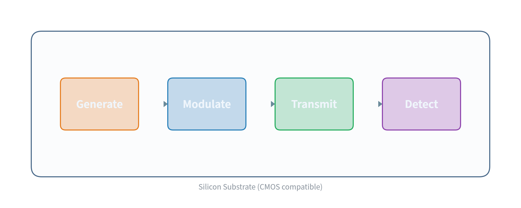
▲ Silicon photonic chip: monolithic integration of light generation, modulation, transmission, and detection
I. Three Material Platforms: Silicon / Indium Phosphide / Thin-film Lithium Niobate
Silicon (Si PICs) wins on CMOS compatibility, high integration density, and low cost – the dominant choice for CPO optical engines; the drawback is that it cannot emit light, requiring heterogeneous integration. Indium phosphide (InP PICs) can emit light directly, but is expensive and incompatible with CMOS. Thin-film lithium niobate (TFLN) provides 110 GHz+ ultra-high-bandwidth modulation, a strong candidate for future high-speed modulation, though heterogeneous integration is challenging. Silicon nitride (SiN) excels in ultra-low-loss, broadband passive waveguides. Real products often combine multiple platforms.
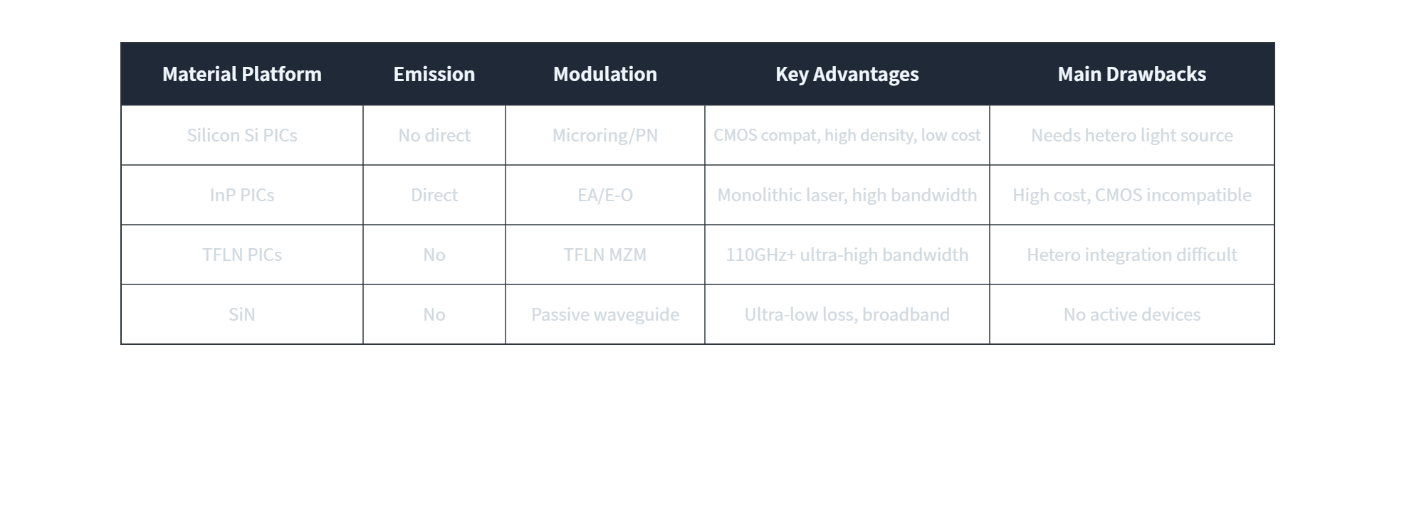
▲ Table 1: Comparison of three major photonic integration material platforms
II. 2025-2026: CPO from PPT to Rack
2.1 Silicon Photonics Enters Mass Production
In 2026, mainstream networking solutions announced full mass production of silicon photonics technology, delivering 5× energy efficiency improvement and 5× AI uptime improvement, providing critical support for exascale AI clusters. AI networking has officially entered the “silicon photonics era”.
2.2 1.6T CPO Chip Debuts
At Hot Chips 2025, the industry showcased the latest progress in co-packaged optics (CPO): a 1.6T CPO chip based on silicon photonics, equipped with microring modulators, delivering high-density optical I/O within a limited package area.
2.3 CPO: From Concept to Production in One Year
In 2026, next-generation compute platforms entered mass production – CPO went from “PPT concept” to “rack reality” in just one year. LPO reduces power by about 30%, while CPO cuts power by over 60%, making it the recognized ultimate solution for high-density AI clusters.
2.4 Market: 10× Growth in Three Years
The CPO market is set to grow from ~$1.5 billion in 2025 to tens of billions of dollars by 2027, with a CAGR exceeding 100%; penetration is expected to rise from less than 1% in 2025 to over 10% in 2027. 2026 is widely regarded as the “first year of 1.6T optical module volume production”.
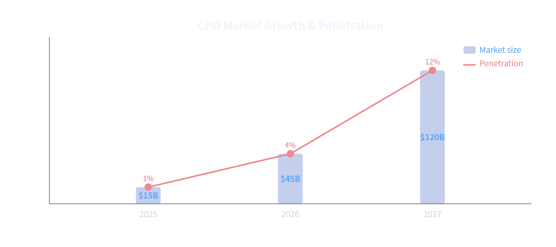
▲ CPO market growth and penetration trend (2025-2027)
III. Core Challenge: Heterogeneous Integration of Light Sources
Since silicon cannot emit light directly, the industry has developed three heterogeneous integration approaches:
Flip-chip bonding – attaching III-V lasers upside down onto the silicon photonic chip, with alignment accuracy within ±0.5 μm, offering the highest yield and currently the mainstream solution;
Micro-transfer printing – using elastomeric stamps to pick and place thousands of tiny III-V devices in parallel, “printing” them onto the silicon substrate, suitable for very large arrays;
Heteroepitaxy – directly growing III-V materials on silicon, the long-term ideal approach but with significant yield challenges.
The yield and cost of laser integration remain the key factors determining whether silicon photonics can truly scale.
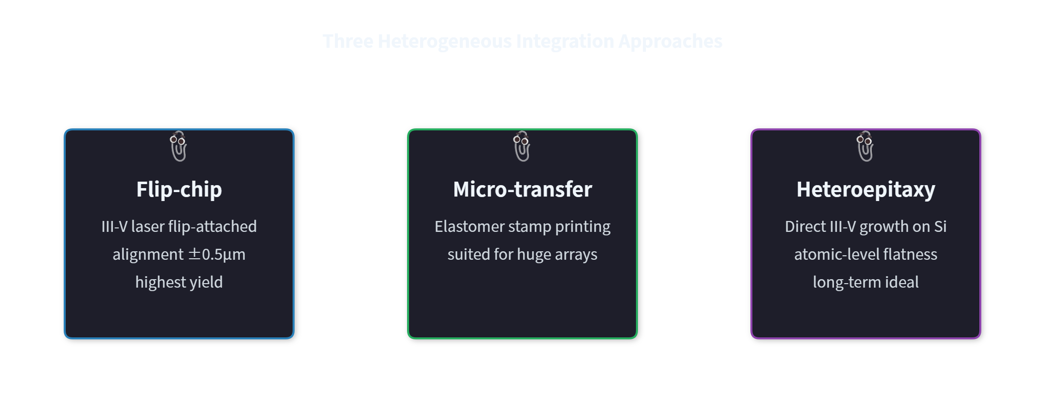
▲ Three heterogeneous integration approaches: flip-chip, micro-transfer printing, heteroepitaxy
IV. Domestic Breakthroughs: Pilot Lines and Industry Chain Rise
Chinese companies already hold over 70% of the global optical module market. Upstream, in silicon photonic chips and pilot line facilities, 2025-2026 saw intensive breakthroughs: multiple 8-inch silicon photonic pilot lines came online, adopting a “1+N” flexible engineering model, offering open pilot runs and advanced R&D support; next-generation silicon photonic production lines are being deployed, driving the shift from “electrically dominated” to “optically dominated” communications. A multi-node domestic silicon photonic ecosystem is taking shape.
V. Application Landscape: From AI Clusters to LiDAR
Silicon photonics is a “platform” technology covering multiple domains: AI data center optical interconnects (CPO 1.6T optical engines), coherent optical communications (coherent transceivers and elastic optical networks), silicon photonic LiDAR (monolithic integration dramatically shrinks size and cost), sensing and biomedical (biosensors, spectral chips), and microwave photonics and optical computing (optical neural network platforms).
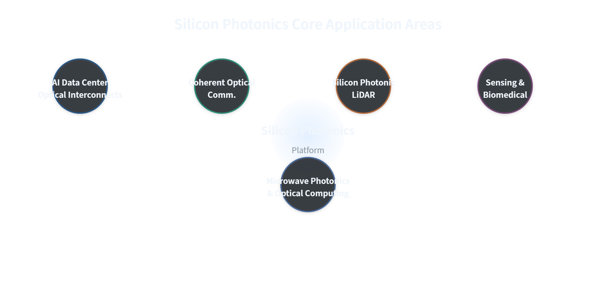
▲ Core application areas of silicon photonics
Platform effect: Silicon photonic chips can integrate TFLN modulators, semiconductor lasers, single-photon detectors, MZI arrays, and many other functional units, serving as a convergence point for multiple technologies in this series.
VI. Summary and Outlook
Silicon photonics integration leverages silicon’s mature processes to carry light’s massive bandwidth, and in facing the physical barrier of “silicon cannot emit light”, it has given rise to ingenious techniques such as flip-chip bonding, micro-transfer printing, and heteroepitaxy.
Looking ahead, three trends are becoming clear:
CPO adoption – from pluggable to LPO to CPO, optical engines move closer to the chip, with mass production in 2026 and scaled deployment in 2027;
standardized foundry – the global silicon photonics industry is shifting from fragmented customization to standardized foundry mass production, driven by foundry platforms;
heterogeneous integrated light sources – III-V/Si and TFLN/Si integration will be the decisive factor; whoever solves laser integration yield and cost first will hold the “heart” of silicon photonics.
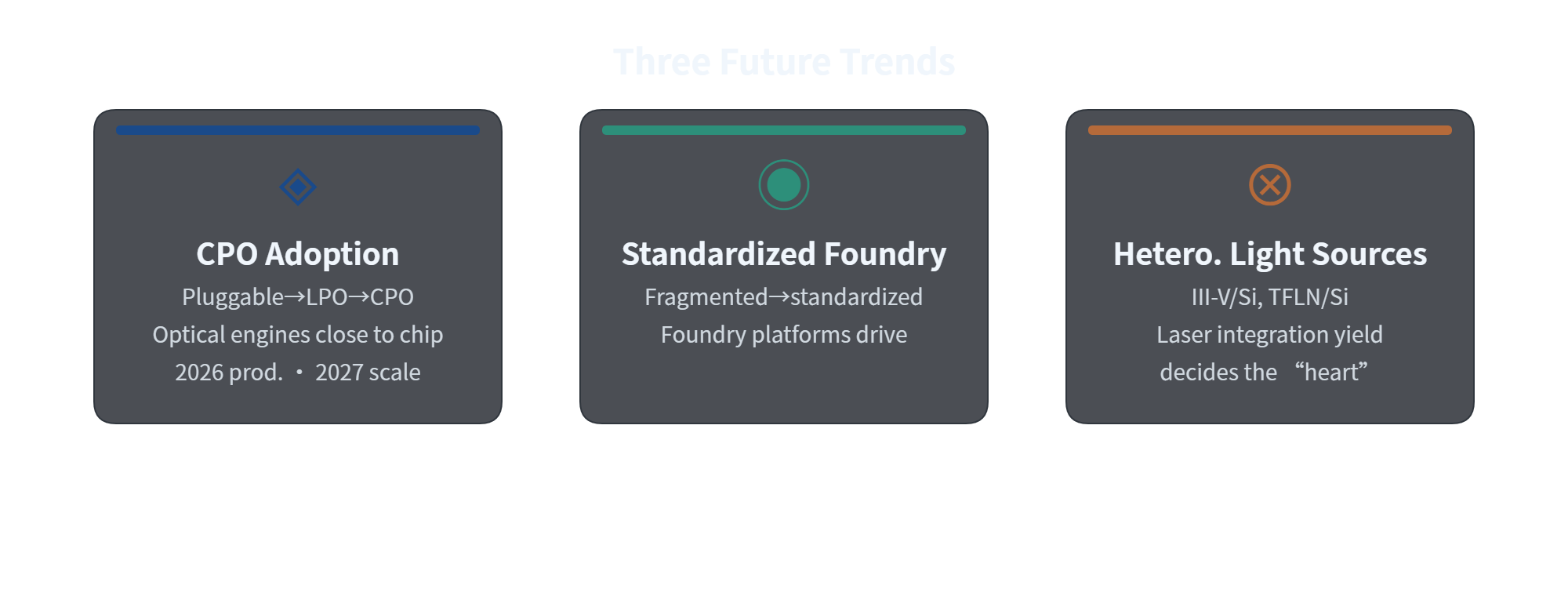
▲ Three major trends: CPO adoption · Standardized foundry · Heterogeneous integrated light sources
When a beam of light is generated, modulated, transmitted, and detected on a silicon chip the size of a fingernail –silicon photonics is pushing the boundary of optical interconnects from the rack to the chip.