
Optical thin films – nanoscale multilayer stacks deposited on optical components (lenses, substrates, chips, etc.) – harness interference between layers to precisely control reflection, transmission, absorption, and polarization. This invisible “armor” enables anti-reflection, spectral splitting, and wavelength division multiplexing. A smartphone camera lens may carry 5–15 layers; a DWDM filter requires 30–100 layers; and a fiber optic gyroscope’s high-reflectance coil demands sub-nanometer thickness precision. The quality of these films directly dictates the performance ceiling and lifetime of any optical system.
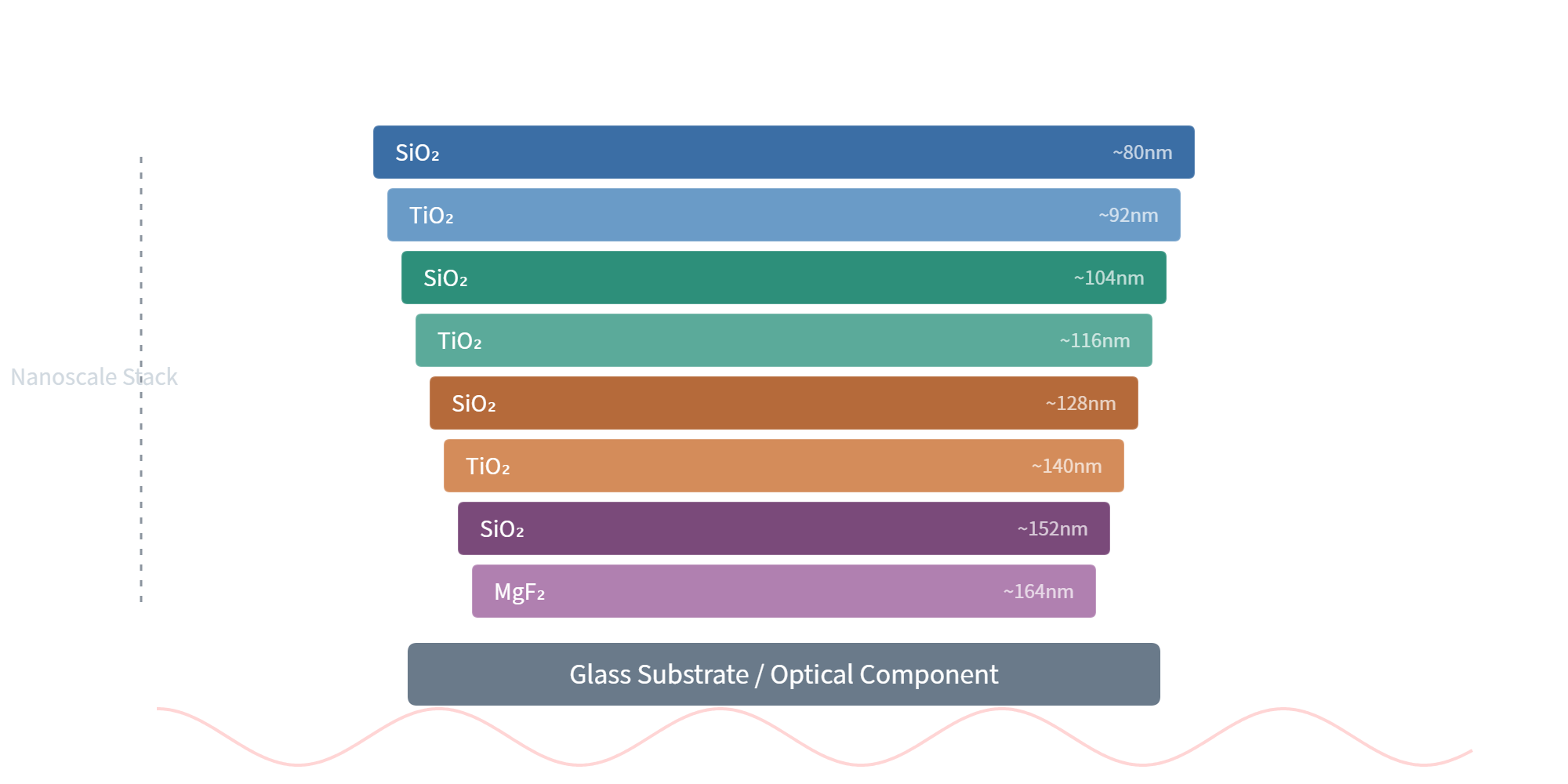
▲ Nanoscale multilayer stack of optical thin films
I. Six Core Film Types
Optical films are categorized by function: anti-reflection (AR), high-reflection (HR), narrow-band filters, transparent conductive oxides, super-hard protective coatings, and advanced metasurfaces. The table below compares materials, processes, key metrics, and applications.
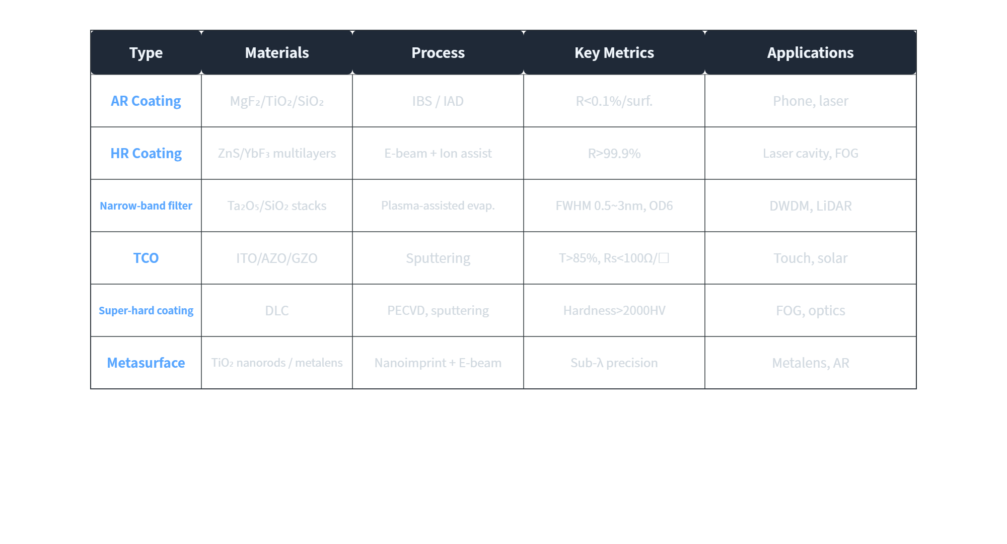
▲ Table 1: Comparison of six core optical thin film types
Anti-reflection (AR) coatings use destructive interference to reduce reflectance from ~4% (air-glass interface) to below 0.1% per surface. High-end phone lenses employ multiple AR layers (MgF₂/TiO₂/SiO₂) to eliminate ghosting and flare. In laser systems, AR coatings are critical – failure can cause back-reflection damage.
High-reflection (HR) coatings exploit constructive interference to achieve >99.9% reflectance, typically using alternating high-index (TiO₂, Ta₂O₅) and low-index (SiO₂, MgF₂) layers. Optimized ZnS/YbF₃ infrared stacks have reduced defect density by an order of magnitude, with absorption below 100 ppm at 164 nm.
Narrow-band filters are essential for DWDM wavelength-selective switches. By precisely controlling layer thickness in SiO₂/Ta₂O₅ stacks, filters achieve FWHM as narrow as 0.5–3 nm (vs. traditional 3–5 nm), with OD6 single / OD8 cemented rejection and <5% transmission drift under humidity (vs. 10–15%).
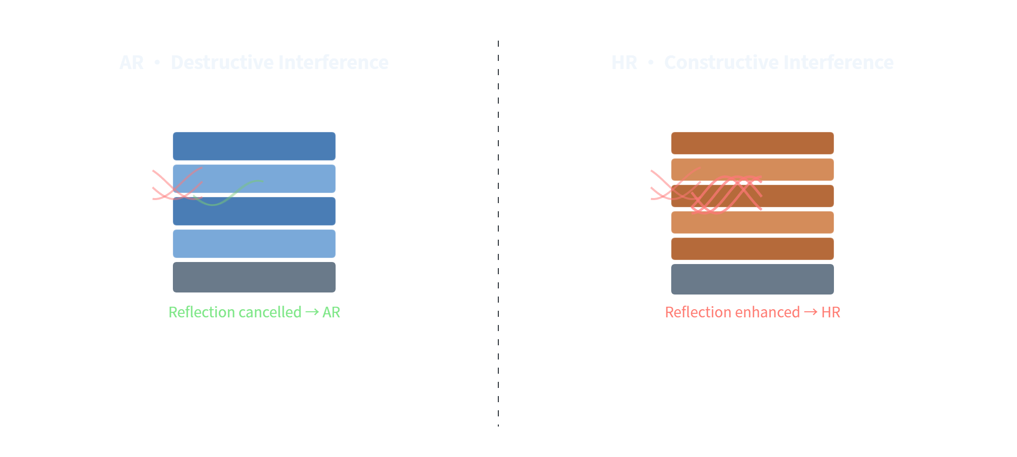
▲ Destructive interference (left, AR) vs. constructive interference (right, HR)
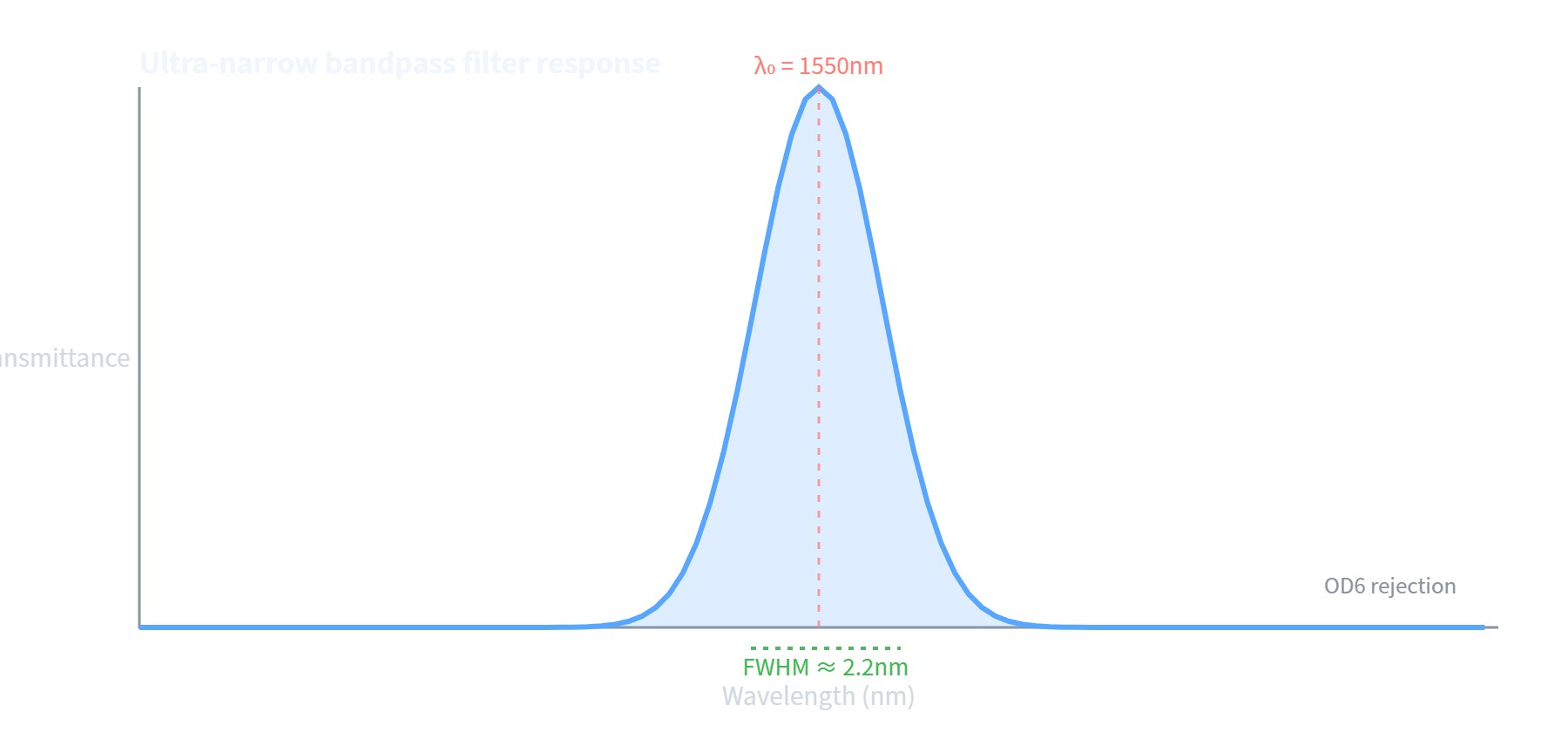
▲ Ultra-narrow bandpass filter response (FWHM 0.5–3 nm)
II. Major Domestic Breakthroughs (2025–2026)
2.1 Infrared Coating Defect Density Reduced by 10×
Infrared films are vital for laser guidance, night vision, and mid-IR communications. By optimizing the deposition of ZnS/YbF₃ multilayers, defect density was cut by an order of magnitude while absorption was held below 100 ppm – reaching world-class level. This is a game-changer for high-volume production of long-wave IR (8–12 μm) systems.
2.2 Full-Portfolio Optical Coating Solutions in Mass Production
In 2026, a comprehensive optical coating portfolio – including AR, HR, and color filters – was unveiled and has entered mass production for leading customers in AI phones, VR headsets, drones, and automotive smart terminals. This marks a critical shift from import dependence to domestic substitution in consumer electronics.
2.3 Metasurfaces: From Lab to Factory
Metasurfaces are 2D arrays of sub-wavelength artificial units that independently control amplitude, phase, and polarization of light in a single layer, potentially replacing bulky stacks of lenses and prisms. In 2025–2026, metasurfaces accelerated towards commercialization: chip-scale UV-visible spin-resolved spectroscopy was demonstrated; a cascaded ultrafast acousto-optic deflector + passive metasurface architecture expanded LiDAR FOV from 2°×2° to 150°×150° while maintaining MHz-class scanning speed, solving the trade-off between speed and field-of-view. Broadband DUV-NIR tunable meta-coatings using inverse design also emerged.
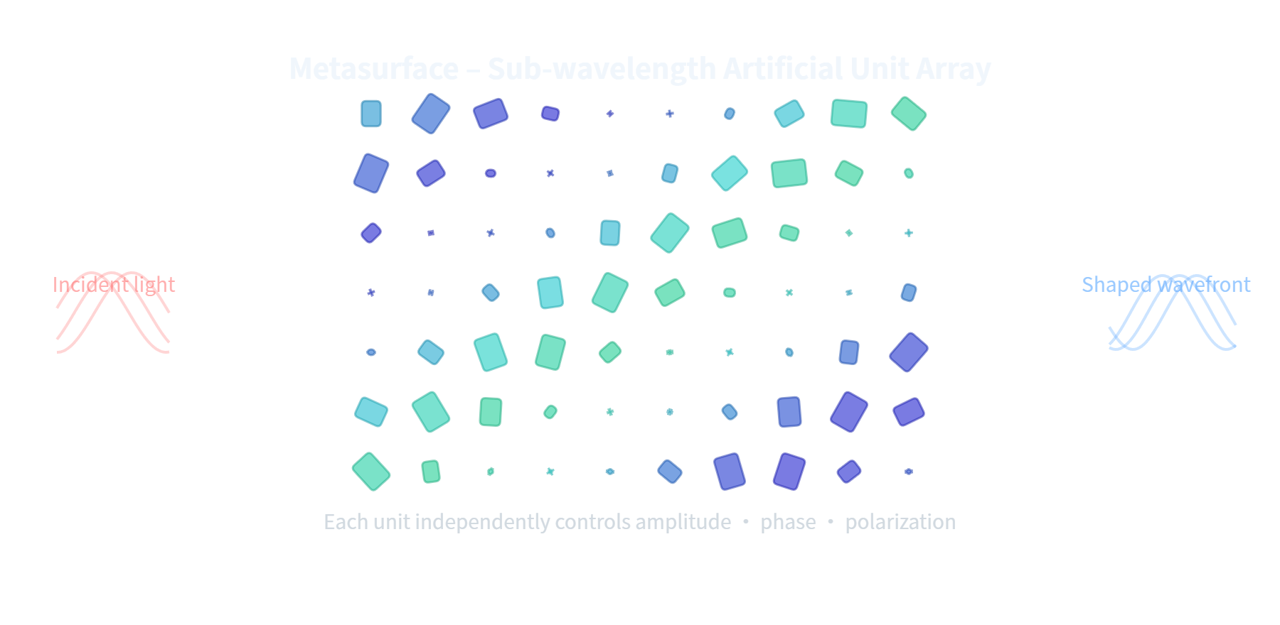
▲ Metasurface: sub-wavelength unit array for single-layer wavefront manipulation
III. Process Technologies: From E-beam to Atomic Layer Deposition
The fabrication process determines film quality, cost, and throughput. Mainstream methods include electron-beam evaporation, magnetron sputtering, PECVD, and atomic layer deposition (ALD).
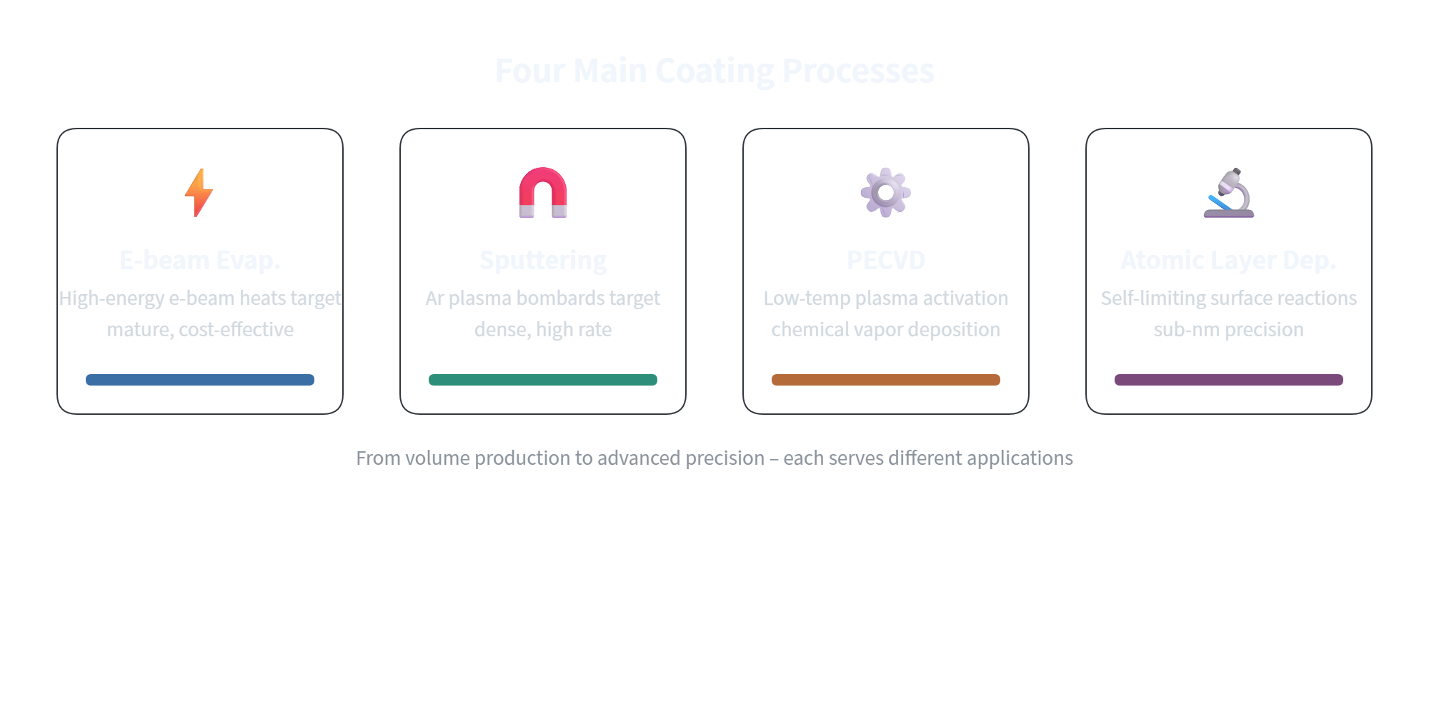
▲ Comparison of four mainstream coating processes
• Electron-beam (E-beam) evaporation – uses a high-energy e-beam to heat and evaporate source materials; mature, cost-effective, and suitable for high-volume production; ion-assisted deposition (IAD) improves film density.
• Magnetron sputtering – bombards a target with Ar plasma to eject atoms; produces dense, adherent films; the go-to process for ITO and DLC hard coatings, and one of the fastest industrial methods.
• Plasma-enhanced chemical vapor deposition (PECVD) – uses low-temperature plasma to drive chemical reactions; ideal for large-area coatings and DLC hard films (hardness >2000 HV).
• Atomic layer deposition (ALD) – self-limiting surface reactions build up films layer-by-layer with sub-nm precision; essential for high-end filters and metasurface fabrication, though slow and costly – mainly for advanced micro-optics.
IV. Application Landscape: Pervasive Across Photonics
Optical thin films are the most “invisible” yet ubiquitous foundation in photonics:
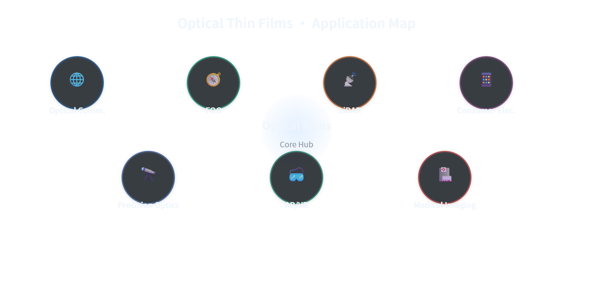
▲ Core application domains of optical thin films
• Optical communications – DWDM interleavers, isolator AR coatings, tunable laser output couplers – the “silent enablers” behind WSS, modulators, and EDFAs.
• Fiber optic gyroscopes (FOG) – DLC protective coatings on fiber coils reduce friction and wear, directly impacting long-term stability.
• LiDAR – 905/1550 nm narrow-band filters (suppress ambient light) and metasurface beam shapers are core to SPAD-SoC and FMCW LiDAR.
• Consumer electronics – waveguide coatings for AR/VR and smartphone AR coatings directly affect user experience.
• Precision optics – multi-layer AR and HR coatings on microscope, telescope, and projector lenses determine image quality.
V. Domestic Localization and Market Landscape
The global high-end optical film market has long been dominated by overseas players with decades of expertise in precision filters and laser-induced damage threshold (LIDT). Domestic players are now catching up across custom filters, IR coatings, consumer-electronics coatings, DLC hard films, ITO etchants, and more.
Localization is not just about components – it involves the entire ecosystem of vacuum equipment (coatings machines, ion sources, thickness monitors) and material supply (high-purity targets, low-absorption glasses). The breakthrough in domestic ALD equipment will be the next critical variable.
Industrial chain depth: From coating machines to high-purity targets, from glass substrates to thickness monitoring – the entire supply chain is being localized. ALD equipment progress will directly determine the cost and scalability of ultra-precision filters and metasurface arrays.
VI. Summary and Outlook
Optical thin films are the most “unseen” battlefield in photonics – nanometre thickness tolerances and ppm-level absorption control define the ultimate performance of every optical component, from communication filters to smartphone lenses.
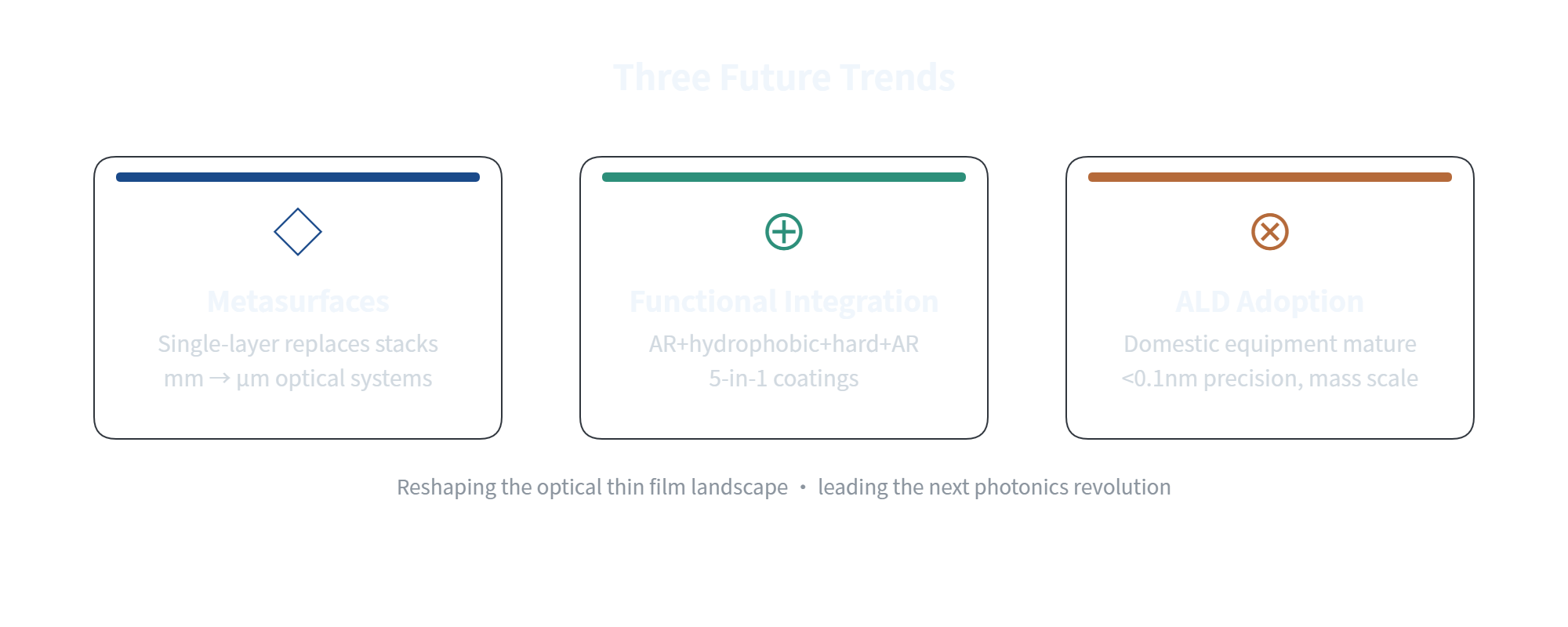
▲ Three major trends: Metasurfaces · Functional integration · ALD Adoption
Looking ahead, three trends will reshape the field:
Metasurface adoption – single-layer metasurfaces replacing multilayer stacks will shrink optical systems from millimeters to micrometers; metalenses are already breaking through in AR and LiDAR.
Functional integration – combining AR, hydrophobic, anti-fingerprint, hard, and augmented-reality functions into 5-in-1 or more coatings will be the next battleground in consumer electronics.
Widespread ALD – as domestic ALD equipment matures, atomic layer deposition will move from labs to mass production, slashing costs for sub-0.1-nm-precision filters and metasurface arrays, paving the way for next-gen optical communications and on-chip photonics.
When a beam of light passes through a carefully engineered nanoscale stack, every joule and every property is orchestrated with precision–optical thin films are the conductors of this symphony.