
1. Why Need an Optical Modulator: Writing “0 and 1” into Light
If the laser is the “light source” of an optical communication system, the optical modulator is its “vocal cord” – it is responsible for writing the information (electrical signals) to be transmitted into the optical carrier. Specifically, the modulator controls the intensity, phase, frequency, or polarization of the output light via an external electrical signal, enabling the light wave to carry data.
Depending on whether the laser itself is modulated, modulation is divided into two categories: Direct Modulation (DML) and External Modulation. Direct modulation modulates the laser drive current directly (as discussed in the second article of this series on directly modulated lasers); it is simple and low-cost, but suffers from frequency chirp and bandwidth limitations at high speeds, making it difficult to support single-lane >100G rates. External modulation extracts continuous wave light from the laser and alters its characteristics with an electrical signal in an external modulator, avoiding chirp – it is the inevitable choice for 800G/1.6T/3.2T high-speed optical modules, with the Mach-Zehnder modulator (MZM) and electro-absorption modulator (EAM) as the mainstream options.
2. Four Technology Routes: From MZM to Silicon PN
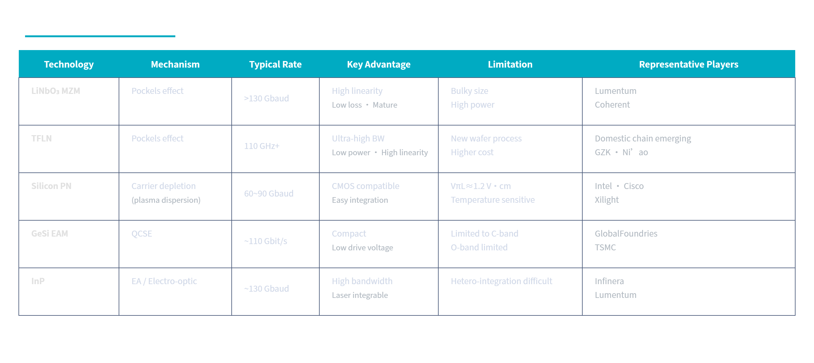
Comparison of four optical modulator technology routes
The Mach-Zehnder modulator (MZM) exploits the Pockels effect of electro-optic materials: an applied voltage changes the waveguide refractive index, altering the phase difference between the two arms, and the interference at the output produces intensity “on/off” switching. Bulk lithium niobate (LiNbO₃) MZMs have been commercially used for decades due to high linearity and low loss.
Thin-film lithium niobate (TFLN) bonds a thin LiNbO₃ film to a silica substrate, leveraging strong optical confinement to reduce modulator size by an order of magnitude, with bandwidths exceeding 110 GHz and symbol rates >130 Gbaud, making it the “must-have” technology for the 1.6T/3.2T era. Silicon PN-junction modulators use carrier-depletion-induced plasma dispersion, are CMOS-compatible and easy to integrate, with symbol rates around 60-90 Gbaud; however, their VπL is about 1.2 V·cm, requiring several millimeters of phase shifter and consuming pJ/bit. Microring-resonator structures can reduce power to 5.3 fJ/bit but have narrow bandwidth (<1 nm) and strict temperature stability requirements. GeSi electro-absorption modulators (EAMs) rely on the quantum-confined Stark effect (QCSE) for compact, low-voltage modulation at ~110 Gbit/s, but are limited to the C-band and cannot operate in the O-band due to Ge’s direct bandgap (~0.7 eV). Indium phosphide (InP) modulators can reach ~130 Gbaud but hetero-integration remains challenging.
3. 2025-2026: A Cluster of Breakthroughs
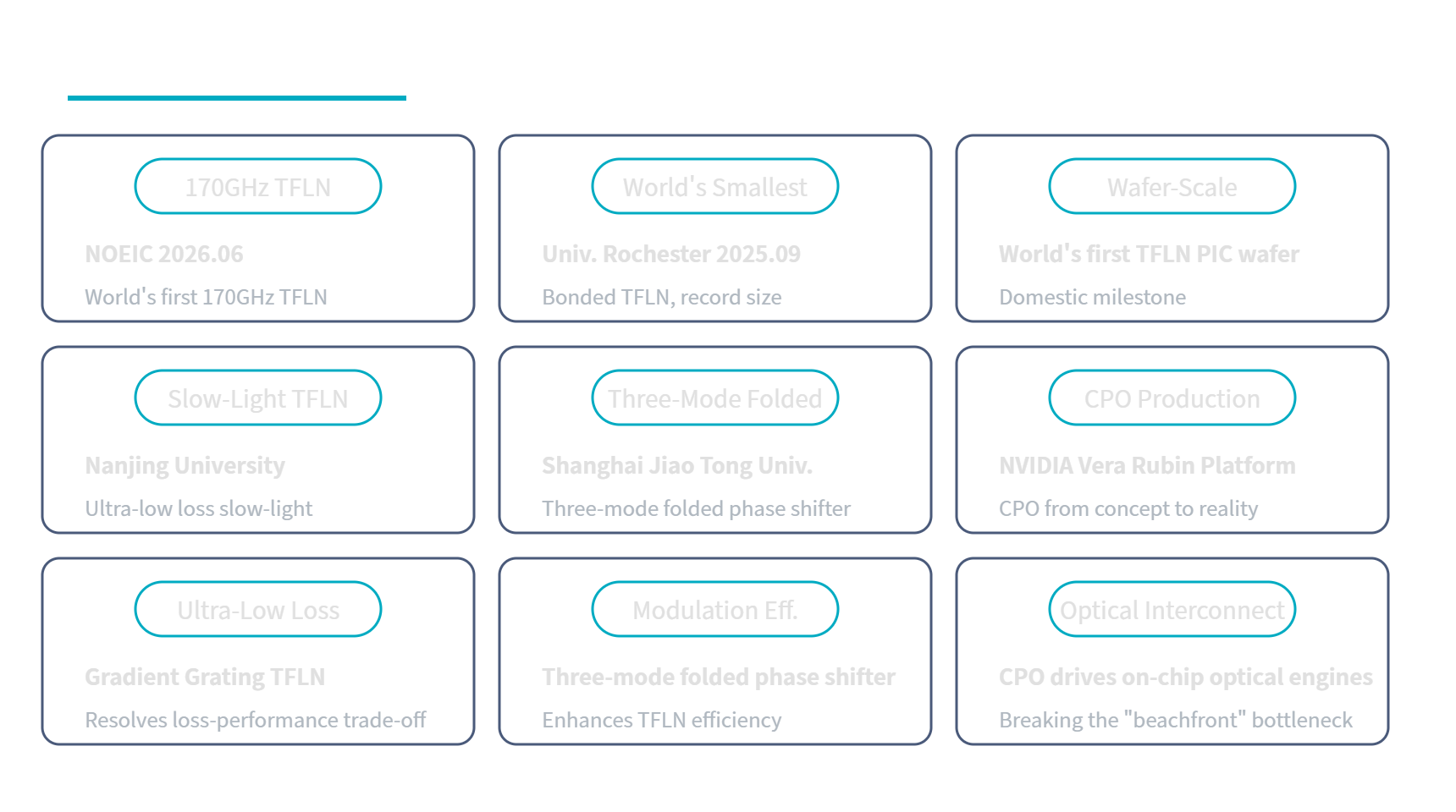
Major breakthroughs in optical modulators (2025-2026)
3.1 Domestic 170GHz TFLN Modulator Tops the Field – In June 2026, the National Optoelectronics Innovation Center (NOEIC) released the industry's first 170GHz thin-film lithium niobate photonic modulator, achieving ultra-high bandwidth with stable low loss on a domestically controlled TFLN platform, providing key support for single-lane 200G/400G ultra-high-speed transmission.
3.2 University of Rochester Creates “World's Smallest Electro-Optic Modulator” – In September 2025, a team at the University of Rochester bonded a thin lithium niobate film on a silica substrate, fabricating the world's smallest electro-optic modulator at that time, with prospects in data communications, microwave photonics, and quantum optics.
3.3 World's First TFLN Photonic Integrated Circuit Wafer Launched – A domestic company achieved the world's first thin-film lithium niobate PIC wafer, marking the transition of TFLN from single-device R&D to wafer-scale manufacturing, clearing key supply chain obstacles for downstream optical module production. In parallel, Nanjing University proposed an ultra-low-loss slow-light TFLN modulator based on gradient gratings, and Shanghai Jiao Tong University reported a three-mode folded phase shifter, further enhancing TFLN modulation efficiency.
4. TFLN: The “Must-Have” Technology for the 1.6T/3.2T Era
The explosion of AI computing power is driving optical modules from 400G and 800G toward 1.6T and even 3.2T. TFLN, with its 110 GHz+ ultra-high bandwidth, ultra-low power consumption, and high linearity, is the optimal solution for single-lane 200G/400G ultra-high-speed modulation. The industry generally regards 2026 as the “first year of scale” for thin-film lithium niobate – by the 3.2T era, TFLN penetration in high-speed optical modules is expected to exceed 40%, with a market CAGR of over 50%. The domestic industrial chain has achieved full coverage from substrate, wafer, to device design, placing China at the same starting line as international giants in the next round of optical interconnect competition.
5. Application Landscape: From AI Data Centers to CPO
The biggest stage for optical modulators is the optical interconnect within AI data centers. According to LightCounting, the global Ethernet optical module market is expected to reach $26.084 billion in 2026, with 800G and 1.6T modules combined penetration increasing by 53.67 percentage points over 2023; by 2028, 3.2T modules will accelerate deployment.
The truly game-changing factor is Co-Packaged Optics (CPO). At the GTC conference in March 2026, NVIDIA announced the full-scale production of the new Vera Rubin platform, and CPO moved from “PPT revolution” to “in-rack reality” in just one year. CPO packages optical engines and switch ASICs on the same substrate, replacing traditional pluggable modules and breaking the “beachfront” bandwidth bottleneck. However, silicon photonic modulators are approaching physical limits, making next-generation modulator breakthroughs (especially TFLN) the key to CPO's large-scale adoption. Optical modulators are also the basic building blocks of MZI meshes in optical computing (as discussed in Article 11), the computing carrier for silicon photonic integration, and the core components of coherent optical communications and microwave photonic systems – they are a “common bridge” connecting multiple photonic technologies.
6. Market Landscape and Domestic Players
The global optical modulator market has long been dominated by international leaders. In 2026, as CPO momentum continued, related industry players saw strong market interest, reflecting high expectations for next-generation modulation and interconnect technologies. On the domestic front, companies such as GZK, Ni’ao Photonics, Xilight, and Huawei are accelerating their catch-up. In the TFLN direction, China has achieved “world-first” breakthroughs at the wafer level, securing a strategic window for domestic high-speed optical modules in the 1.6T/3.2T era.
7. Summary and Outlook
The history of optical modulators is an engineering saga of continuously challenging the “bandwidth-power-size” triangle. From bulky bulk-lithium-niobate devices to chip-scale ultra-high-bandwidth TFLN; from CMOS-compatible silicon photonics integration to CPO bringing optical engines onto switch chips – each leap redefines the speed and energy-efficiency limits of optical interconnects.
Looking ahead, three clear trends emerge:
TFLN Adoption: As wafer manufacturing matures and costs decline, TFLN will penetrate from high-end coherent communications to full 800G/1.6T/3.2T scenarios, gradually becoming the “default” choice for high-speed modulation.
CPO Co-Packaging: As silicon photonic modulators approach physical limits, heterogeneous integration of TFLN with silicon photonics will become the critical path for CPO advancement, pushing optical interconnects from “pluggable” to “on-chip co-packaged.”
Opto-Electronic Integration: Co-design of modulators with lasers, detectors, and driver-TIAs will enable monolithic optical engines, providing ultra-high bandwidth density and low-power interconnect substrates for AI clusters and optical computing.
When the intensity and phase of a light beam can be precisely controlled at the picosecond level by a chip, and when “0s and 1s” are written into the optical carrier at trillion-bits-per-second rates – the optical modulator is precisely the beating heart of this optical interconnect revolution.