
From MZI Matrix Multiplication to LightGen All-Optical Generative Chips · 2026 Frontiers and Industry Landscape.
Optical computing (photonic computing) uses photons instead of electrons for information processing, breaking through the “power wall” and “memory wall” of electronic chips. Moore’s Law is approaching physical limits – the 450 W TDP of NVIDIA H100 exposes three structural contradictions: thermal density, memory bottleneck, and process limits. Photons inherently offer speed of light propagation, zero resistive heating, and massive parallelism, enabling orders-of-magnitude performance gains in matrix multiplication – the core workload of AI.
1. Why Matrix Multiplication: The Core Battlefield
Matrix-vector multiplication (MVM) accounts for 70-90% of the computation in deep neural networks. When light passes through a mesh of Mach-Zehnder interferometers (MZI), interference and coupling naturally perform matrix multiplication entirely in the optical domain, with no data movement and ultra-low energy. An MZI forms a 2×2 unitary transformation; large meshes can implement arbitrary complex matrices. Speed is limited only by the propagation time of light (picoseconds), with no static power consumption. The larger the AI model, the more pronounced the parallel advantage of optical computing.
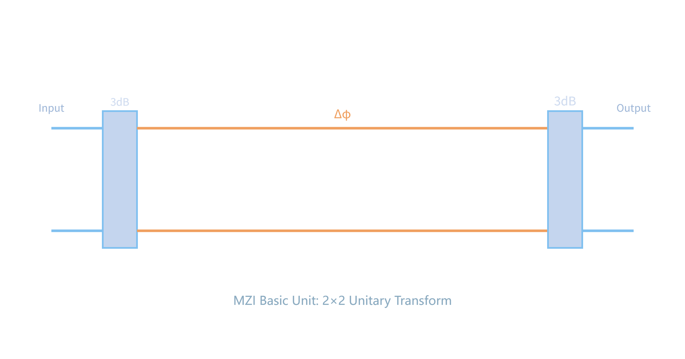
MZI basic unit: two 3-dB couplers + phase-shift arms, performing 2×2 unitary transform
2.Five Technology Routes: Each with Its Strengths
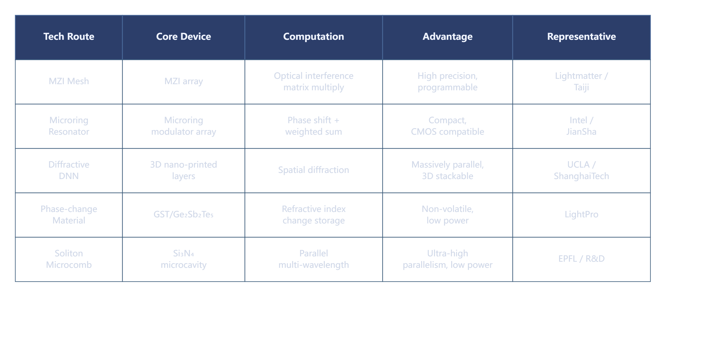
Table 1: Comparison of five major optical computing technology routes
3. Major Breakthroughs in 2025-2026
3.1 Science Cover: LightGen – World’s First All-Optical Generative AI Chip
In December 2025, the group of Chen Yitong at Shanghai Jiao Tong University published in Science the world’s first all-optical chip supporting large-scale semantic visual generation – LightGen. It integrates over 2 million photonic neurons on a single chip, performs end-to-end optical signal processing (zero optoelectronic conversion), and uses a training algorithm that does not rely on ground truth. It achieves ~100× speed and energy efficiency over top-end digital chips in high-resolution image synthesis, 3D generation, and video generation.
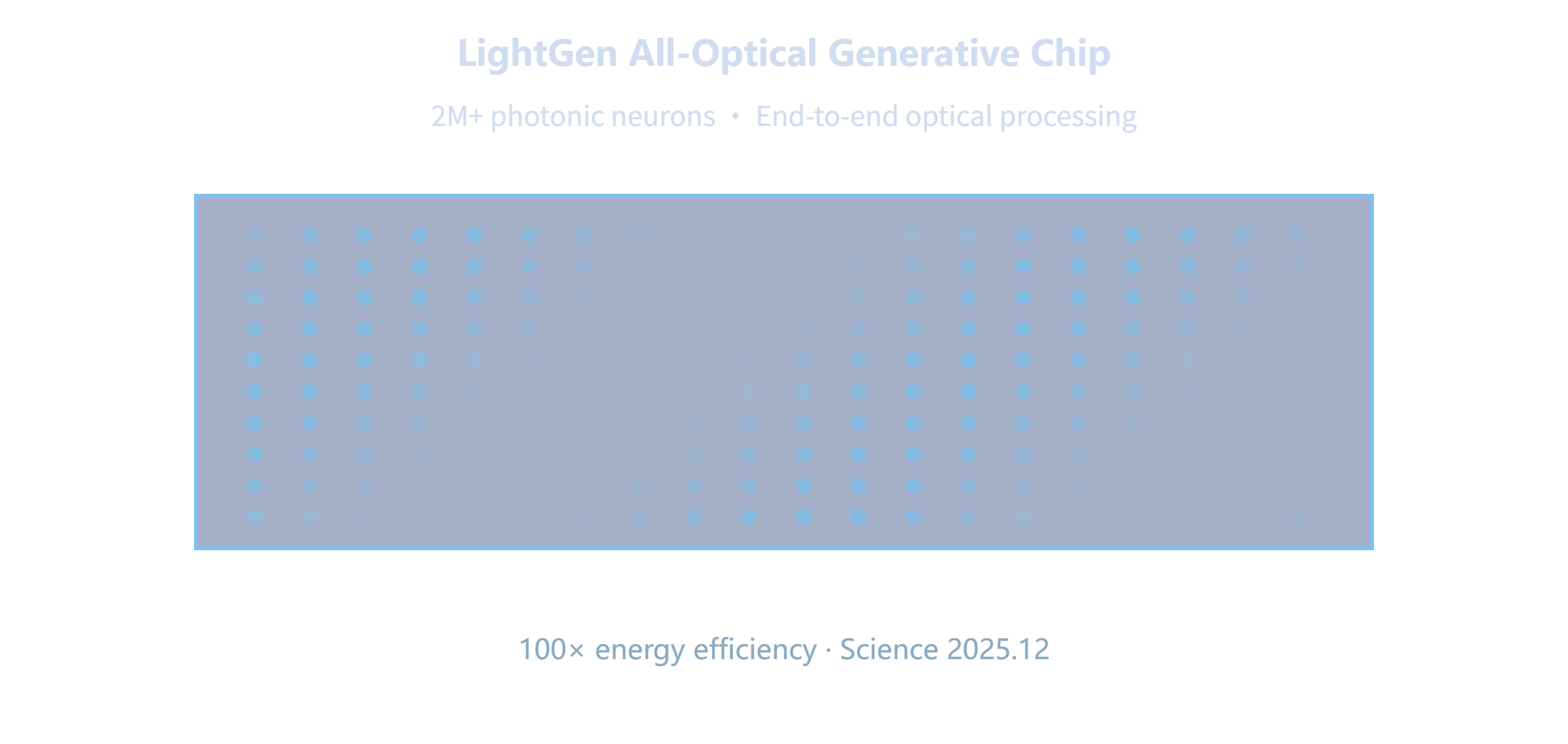
LightGen all-optical generative chip: 2M+ photonic neurons, end-to-end optical processing
3.2 Tsinghua “Taiji-II”: First Optical Training
In 2026, the groups of Fang Lu and Dai Qionghai at Tsinghua University published “Taiji-II” in Nature, introducing a fully forward optical training architecture that enables in-situ training of large-scale neural networks on photonic chips for the first time – breaking the limitation that optical chips could only perform inference.
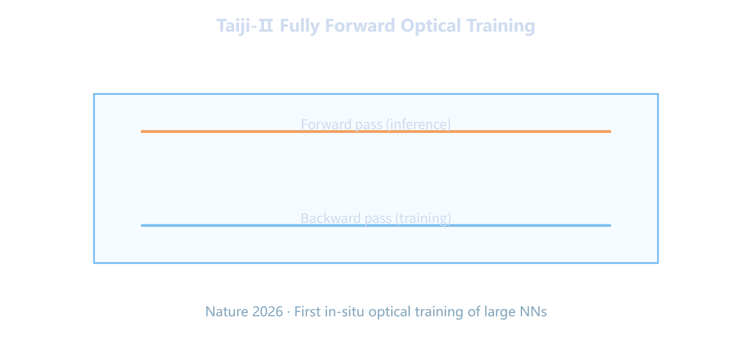
Taiji-II: fully forward optical training architecture filling the gap in optical training
3.3 Glass-Substrate Optical Chip: kTOPS/W Energy Efficiency
Guangbenwei Technology is developing a glass-substrate optical computing chip with lower optical loss and better thermal stability than silicon, theoretically reaching kPOPS compute and kTOPS/W energy efficiency (NVIDIA H100 ~0.13 TOPS/W), targeting the AI inference market, which is expected to account for 75% of AI compute by 2030.
Glass-substrate optical chip: lower loss, higher energy efficiency
4. Representative Achievements at a Glance
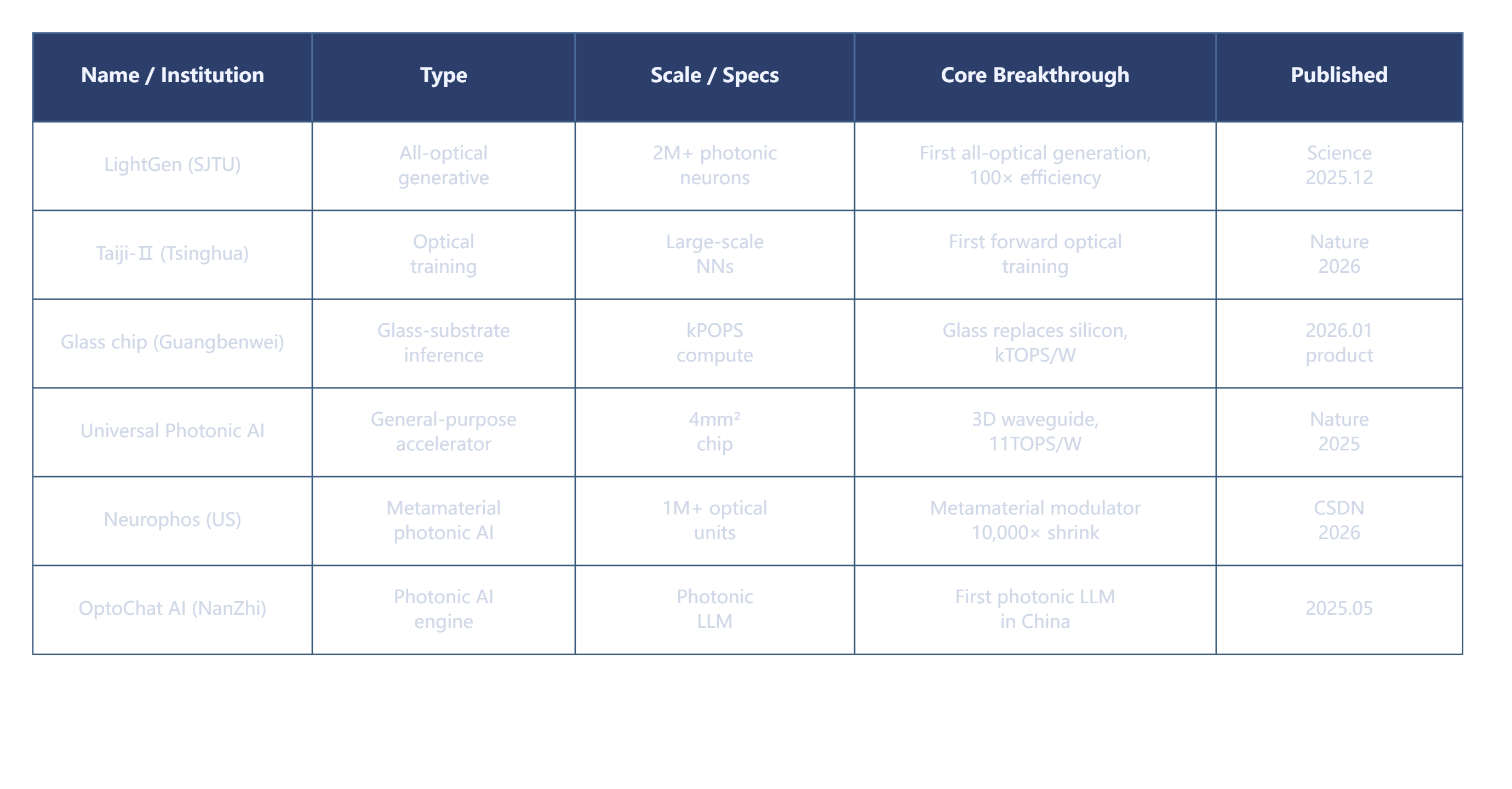
Table 2: Representative optical computing achievements in 2025-2026
5. Commercialization and Industry Ecosystem
International: NVIDIA invests in Ayar Labs (optical interconnects); Lightmatter’s photonic AI accelerator consumes 1/9 the energy of electronics; Neurophos uses metamaterials to shrink modulators 10,000×, integrating millions of optical units on a single chip.
Domestic (China): The Wuxi Photonic Chip Pilot Line (SJTU) started in 2024; NanZhi Optoelectronics released China’s first photonic LLM, OptoChat AI; thin-film lithium niobate (TFLN) is becoming a key enabling material.
Challenges: Precision (FP32 still needs breakthrough), on-chip laser integration, mass production, and lack of mature training toolchains.
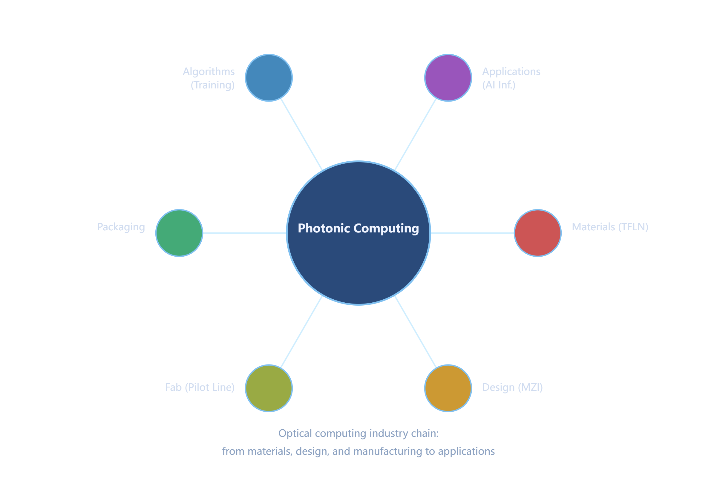
Optical computing industry chain: from materials, design, and manufacturing to applications
6. Summary and Outlook
Optical computing will not replace electronics entirely, but will serve as a “specialised accelerator” for AI. Three major directions over the next decade: ① from inference to training (Taiji-II has opened the door); ② from cloud to edge (chip-scale optical modules for low-power edge AI); ③ hybrid photonic-electronic integration (optical for matrix multiplication, electronics for control and storage). LightGen on the cover of Science may mark the true beginning of the “photonic computing era”.
Conclusion
When the growth of computing power is constrained by the physical limits of electrons, photons open a new window. Optical computing is moving from labs to data centres, from inference to training, from research to industry. LightGen, Taiji-II, glass-substrate chips - each breakthrough redefines the limits of compute at the “speed of light”. In the coming decade, optical and electronic computing will coexist and cooperate, sustaining the exponential growth of AI compute.