
PPLN Waveguide Devices: The “Optical Wavelength Bridge” for Quantum Internet and Gas Spectroscopy—— From Quasi-Phase Matching to Integrated Quantum Light Sources
I. The “Soul of Nonlinear Optics”: Physical Essence of PPLN Waveguides
In the precise toolbox of optoelectronics, the periodically poled lithium niobate (PPLN) waveguide occupies an exceptionally special position – it serves as the “bridge” connecting different wavelength photonic worlds in the quantum internet, and as the “magic prism” that turns the invisible into visible in gas spectroscopy.
To understand why PPLN is so important, we must go back to the fundamentals of nonlinear optics. Lithium niobate (LiNbO₃) is one of the materials with the highest known nonlinear coefficients, with a second-order nonlinear coefficient d₃₃ as high as ~27 pm/V – meaning that when intense light propagates through the crystal, the strong second-order nonlinear response allows photons to exchange energy, producing second-harmonic, sum-frequency, and difference-frequency effects.
However, in ordinary lithium niobate, dispersion causes the fundamental and second-harmonic waves to travel at different speeds (phase mismatch), preventing efficient energy transfer. The revolutionary design of PPLN lies in its periodic poling: a high-voltage poling process flips the spontaneous polarization direction every few micrometres, creating a grating-like periodic structure – this quasi-phase matching (QPM) exactly compensates for the phase mismatch, drastically enhancing nonlinear conversion efficiency, reaching >70% in centimetre-long waveguides.
PPLN waveguides confine this nonlinear process to a micron-scale cross-section, achieving extremely high power density while supporting direct fibre-coupled input/output – a triple advantage of high efficiency, low threshold, and engineering integration that underpins its transition from laboratory to practical quantum communication and gas sensing.
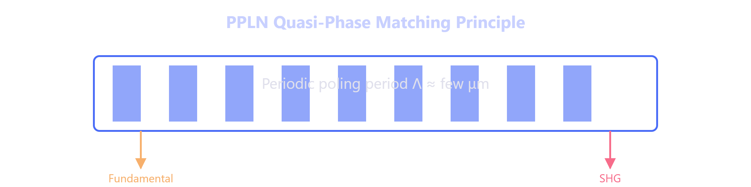
Figure 1: PPLN periodic poling structure and quasi-phase matching
II. Nonlinear Frequency Conversion: The Core Magic of PPLN
2.1 Four Basic Conversion Mechanisms
PPLN waveguides support four fundamental nonlinear processes, each with distinct applications:
Second-harmonic generation (SHG): Two photons of the same frequency combine to produce a photon at double the frequency – e.g., 1550 nm → 775 nm, used for rubidium atom cooling and quantum memory.
Sum-frequency generation (SFG): Two different wavelengths produce a shorter wavelength – e.g., 1550 nm + 1064 nm → 633 nm.
Difference-frequency generation (DFG): The difference of two frequencies yields a new lower frequency – essential for generating mid-IR (2–5 μm) laser light for gas sensing.
Optical parametric down-conversion (OPD/OPG): A pump photon splits into two lower-energy photons (signal and idler) – the standard method for producing entangled photon pairs.
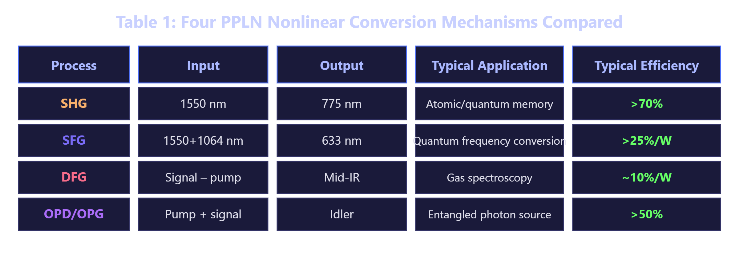
Figure 2: Comparison of four nonlinear conversion mechanisms
2.2 From Telecom to Atomic Physics: A Wavelength “Translator”
One of the most critical applications of PPLN waveguides in quantum technology is as a “wavelength translator” for quantum networks. Different subsystems operate at different standard wavelengths – e.g., silicon-spin qubits at ~900 nm, while fibre-based quantum communication uses 1550 nm.
A PPLN-based quantum frequency converter (QFC) can shift a photon’s wavelength while preserving its quantum state (entanglement, superposition, etc.), enabling interconnection between otherwise incompatible quantum nodes. In 2025, a team in China demonstrated quantum teleportation using a PPLN QFC to convert communication-band single photons to the target wavelength – a key milestone for the quantum internet.

Figure 3: PPLN as a quantum frequency converter connecting different wavelength nodes
III. Quantum Entangled Light Sources: The Quantum Advantage of PPLN
3.1 Shandong University: Broadband Quantum Photon Source with Step-Chirped PPLN
In 2026, a team from Shandong University reported a broadband quantum photon source based on step-chirped PPLN waveguides. By segmenting the poling period along the waveguide, they achieved wideband quasi-phase matching, allowing a single chip to efficiently convert multiple wavelengths simultaneously, greatly enhancing frequency flexibility for quantum networks.
3.2 Shanghai Jiao Tong University: Time-Bin Entanglement and Multi-User Quantum Fusion Networks
The team of Chen Xianfeng and Zheng Yuanlin at SJTU has been a leading force in PPLN-based quantum photonics.
In 2025, they developed a multi-user quantum communication network using time-bin entanglement and Bell-state measurements, enabled by PPLN wavelength conversion. Later that year, they demonstrated entanglement swapping across independent networks, published in Nature Photonics – a major breakthrough for scalable quantum networking.
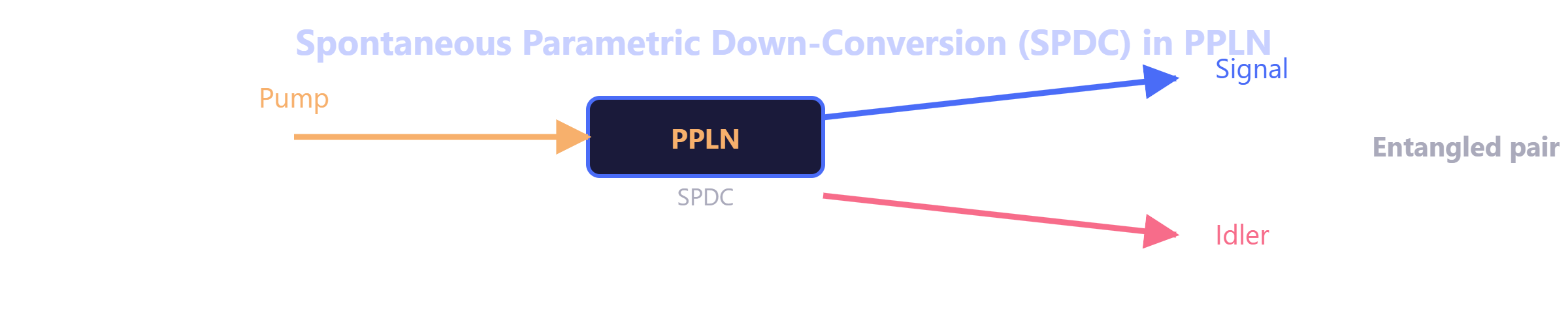
Figure 4: SPDC in PPLN producing polarization-entangled photon pairs
3.3 USTC: Electrically Pumped, On-Chip High-Brightness Entangled Source
In December 2025, a team led by Pan Jianwei and Zhang Qiang at USTC demonstrated the first electrically pumped, on-chip integrated high-brightness polarization-entangled photon source. They hybrid-integrated a 780 nm DFB laser with a thin-film lithium niobate photonic chip, achieving a brightness six orders of magnitude higher than previous silicon-nitride platforms, with a bandwidth of 73 nm and Bell-state fidelity >96%, in a 15×20 mm² device – a critical step toward practical integrated quantum sources.
3.4 Sun Yat-sen University: Micro-Nano Entangled Photon Source
In 2025, a team from Sun Yat-sen University reported in Nature a cavity-enhanced spontaneous double-photon emission scheme, achieving a two-photon fidelity of 99.4%, providing a key device for on-chip quantum information processing.
IV. Gas Spectroscopy: PPLN Sees the Invisible
4.1 Why PPLN for Mid-IR Gas Detection?
Most gas molecules (CH₄, CO₂, CO, NH₃, etc.) have strong characteristic vibrational absorptions in the mid-IR (2–5 μm) – the molecular “fingerprint” region, offering the highest selectivity for gas sensing. However, commercial mid-IR lasers are immature, incomplete in wavelength coverage, and expensive.
PPLN-based difference-frequency generation provides a practical path: two near-IR pump lasers (e.g., 1550 nm and 1064 nm) are mixed in a PPLN waveguide to output tunable mid-IR light. By tuning one pump, the mid-IR wavelength can be continuously scanned across the absorption lines of multiple gases.
A typical scheme uses a 1550 nm tunable telecom laser and a fixed 1064 nm laser to generate 3–5 μm light, covering CH₄ (3.3 μm), CO₂ (4.2 μm), CO (4.6 μm), etc. Single-channel sensitivity reaches ppb levels, and with cavity enhancement, even ppt levels are achievable.

Figure 5: PPLN difference-frequency generation for mid-IR laser gas sensing
4.2 Entangled Dual-Comb Spectroscopy (EDCS)
In 2025, EDCS emerged as a new frontier – using quantum correlations in entangled frequency combs to suppress noise below the shot-noise limit, enabling ultra-sensitive remote gas sensing and chemical imaging.
4.3 Mid-IR Supercontinuum and Frequency Combs
In 2025, researchers generated supercontinuum from 330 nm to 2400 nm in PPLN microwaved waveguides, along with self-referenced frequency combs, enabling simultaneous multi-component analysis.
V. Optical Frequency Combs: PPLN’s Role in Precision Metrology
Optical frequency combs serve as “optical rulers” linking microwave and optical frequencies. In the 1550 nm band, PPLN-based comb modules are commercially available with 25 GHz spacing and C-band coverage. In 2026, EPFL’s Kippenberg group demonstrated a 10 GHz integrated soliton microcomb in silicon nitride, breaking the low-repetition-rate barrier and opening new opportunities for integrated combs in quantum metrology and optical communications.

Figure 6: Optical frequency comb principle
VI. Commercial PPLN Waveguide Devices: From Research to Industry
6.1 Global Suppliers and Product Landscape
The global PPLN market offers both research-grade and industrial products, with suppliers such as Covesion (UK), HCP (Germany), and various custom providers. Key specifications include conversion efficiency (%/W), wavelength range (350–5000 nm), waveguide type (buried vs. ridge), temperature tuning range, and fibre-coupling loss.
6.2 Application-Specific Selection Guide
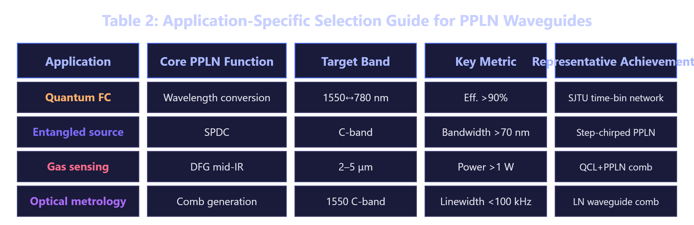
Figure 7: Application-specific selection guide for PPLN waveguide devices
For quantum communication users, the 1550 nm telecom band is the top priority – lowest fibre loss (0.2 dB/km), full compatibility with existing infrastructure, and highest InGaAs single-photon detector efficiency (>80%). PPLN serves as the wavelength bridge to connect with atomic quantum memories (780/795 nm) or silicon-spin qubits (~900 nm).
VII. Conclusion and Outlook: From Material to Quantum Internet
PPLN waveguides are among the most “bridge-building” devices in contemporary quantum optoelectronics. They unite the high nonlinearity of lithium niobate, the engineering flexibility of quasi-phase matching, and the high power density of waveguide confinement, offering a complete chain from theory to application in quantum communication, computing, gas spectroscopy, and precision metrology.
From the perspective of the quantum internet, PPLN as a quantum frequency converter solves the “language barrier” between heterogeneous quantum nodes – different wavelengths and platforms can be interconnected via PPLN translation. The multi-user entanglement swapping and network fusion demonstrated by SJTU represent an early prototype of this vision.
Looking ahead, PPLN technology will evolve along three directions: (i) thin-film lithium niobate (TFLN) integration – QPM on TFLN reduces drive voltage and enables more compact chip-scale devices; (ii) multi-channel and arrayed waveguides – to support parallel wavelength-division quantum operations; and (iii) fully integrated quantum photonic integrated circuits (QPIC) – combining PPLN with lasers, detectors, and modulators on a single chip, the ultimate goal for large-scale quantum technologies.