
I. The Optical Interconnect Bottleneck – The Data Center Dilemma in the Age of AI
Over the past three years, the parameter scale of large language models has expanded tenfold annually. From GPT-3’s 175 billion parameters to GPT-4 crossing the trillion-parameter threshold, and by 2025, multiple vendors racing to release trillion- to tens-of-trillions-parameter multimodal models, the demand curve for AI compute far outpaces the trajectory Moore’s Law can depict.
The foundation of compute power is GPU clusters, and the real-time exchange of massive data between GPUs is becoming the core bottleneck limiting overall AI system efficiency. In a data center with a 10,000-GPU cluster, the communication bandwidth requirement per GPU has reached 800 Gbps or even 1.6 Tbps; the total data transferred across servers and racks exceeds hundreds of petabytes per day. This means traditional copper electrical interconnects have hit physical limits in power consumption, bandwidth-distance product, and latency — optical interconnect has shifted from an “option” to the “only way forward.”
LightCounting’s 2025 forecast clearly reveals this trend: the global Ethernet optical module market will reach $26.084 billion in 2026, with 800G and 1.6T modules penetrating 53.67 percentage points more than in 2023. More aggressively, research institutions have pointed out that 3.2T optical modules will require single-channel modulation rates of 400 G class to meet future AI cluster communication needs — and this is precisely the core driver for Thin-Film Lithium Niobate (TFLN) technology to enter the stage.
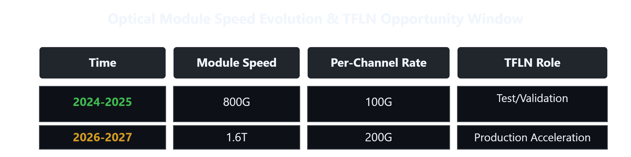
Figure 1: Optical module speed evolution & TFLN opportunity window.
II. TFLN Technology – Why It Becomes the Answer for Next-Gen Optical Modulation
2.1 From Bulk to Thin Film – A Revolution in Physical Structure
Traditional lithium niobate modulators are fabricated from bulk material, with waveguide widths of 5-10 μm and half-wave voltage Vπ of 5-7 V, leading to high power consumption. Thin-Film Lithium Niobate (TFLN) bonds a few hundred-nanometer-thick single-crystal film onto a silicon dioxide substrate, compressing waveguides to 1-3 μm, Vπ below 3 V, reducing drive power by over 40%, and shortening device length from 60-100 mm to less than 40 mm.

Figure 2: Bulk lithium niobate vs. TFLN structure comparison.
2.2 Competitive Landscape of Three Modulator Material Platforms
Silicon photonics: Mature CMOS process, low cost, but modulation efficiency is moderate; per-channel rate 60-90 Gbaud.
Indium phosphide (InP): Can reach >130 Gbaud, but wafer size is small and cost is high.
Lithium niobate (TFLN): Best Pockels effect, bandwidth >60 GHz (some >100 GHz), low Vπ, excellent linearity.
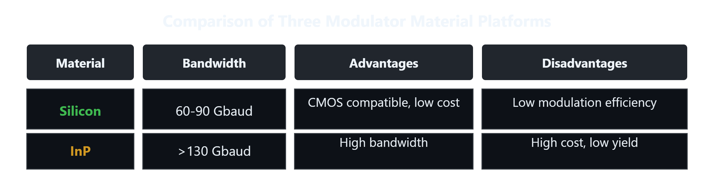
Figure 3: Comparison of three modulator material platforms.
2.3 TFLN Modulator Product Portfolio
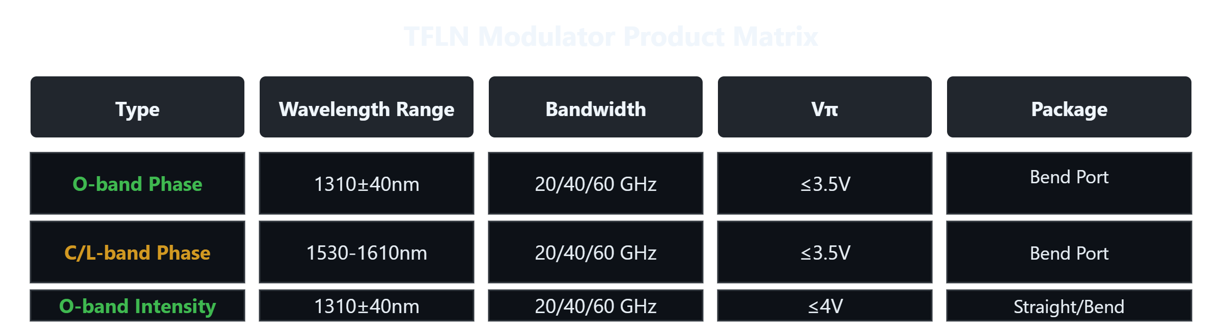
Figure 4: TFLN modulator product matrix.
III. 2025-2026 Industrialization Breakthroughs – TFLN from Lab to Volume Production
3.1 World’s First 8-inch Silicon-Photonic TFLN Optoelectronic Integrated Wafer
In 2026, the Jiufengshan Laboratory, in collaboration with industry partners, successfully produced the world’s first 8-inch silicon-photonic thin-film lithium niobate optoelectronic integrated wafer, bonding an 8-inch SOI silicon-photonics wafer with an 8-inch LN wafer, integrating both optical transmission and reception functions on a single chip. At nearly the same time, the Wuxi Photonics Chip Institute (CHIPX) of Shanghai Jiao Tong University announced that its 6-inch TFLN photonic chip pilot line commenced production in June 2025, achieving volume manufacturing with ultra-low loss and ultra-high bandwidth.
3.2 TFLT Heterogeneous Integration – A Strong Competitor to TFLN
In May 2025, a joint team from the Shanghai Institute of Microsystem and Information Technology (SIMIT), EPFL, and KIT published in Nature a thin-film lithium tantalate (TFLT)-on-silicon-nitride heterogeneous photonic chip, achieving 333 Gbit/s intensity modulation and 581 Gbit/s coherent IQ modulation with a 3-dB bandwidth of ~100 GHz, positioning TFLT as a strong competitor to TFLN.
3.3 Harvard Team – First Integrated High-Power Laser on TFLN Chip
In 2026, a Harvard SEAS team, together with Freedom Photonics and HyperLight, demonstrated the world’s first fully integrated on-chip high-power laser on TFLN, achieving >60 mW output power while maintaining 50 GHz electro-optic modulation performance, paving the way for fully integrated TFLN transmitters.
3.4 Quantum Entanglement and Inverse Design – TFLN Breakthroughs in Quantum Photonics
ETH Zurich demonstrated a programmable quantum entanglement circuit on TFLN with spectral brightness of 26 MHz·nm⁻¹·mW⁻¹ and Bell-state fidelity >90%. Meanwhile, Nature Communications reported inverse-design ultra-compact photonic devices on TFLN (mode multiplexer 19×25 μm², bend radius 30 μm) integrated with high-speed modulators, achieving 120 Gbps per channel.
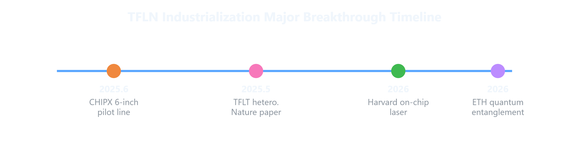
Figure 5: TFLN industrialization major breakthrough timeline.
IV. Market Opportunity – From 800G to 3.2T, TFLN Enters the Adoption Window
According to LightCounting, the 3.2T optical module market will reach ~$1.396 billion in 2028 and exceed $24 billion by 2031. Single-channel modulation rates need to jump from 100G to 400G, and TFLN, with its high modulation efficiency, low drive voltage, and excellent linearity, is viewed as the core candidate for 3.2T. It is estimated that the TFLN modulator market could reach ~3 billion RMB by 2031, with a CAGR of 271% from 2029 to 2031.
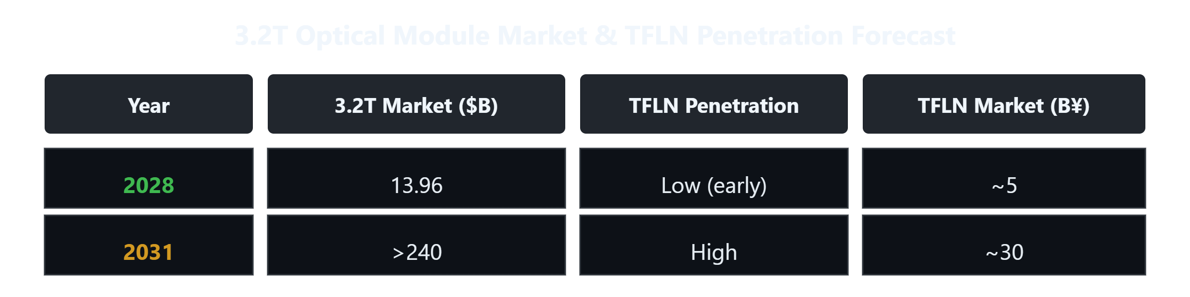
Figure 6: 3.2T optical module market & TFLN penetration forecast.
V. Future Outlook – TFLN and the Road to Photonic Integration
TFLN technology is advancing along two main tracks:
Heterogeneous integration: Harvard’s on-chip laser demonstration points the way to monolithic integration of lasers, modulators, multiplexers, and detectors, fundamentally changing transmitter design.
Hybrid integration: Combining silicon-photonics / silicon-nitride passive waveguides with TFLN/TFLT electro-optic modulation, balancing performance and manufacturability.
With the continuous explosion of AI compute demand, the gradual ramp-up of photonic chip pilot lines, and the maturing of heterogeneous integration, TFLN is rapidly evolving from a “promising new technology” into the core infrastructure for next-generation ultra-high-speed optical interconnects.

Figure 7: TFLN future integration roadmap.