
Photodetectors are semiconductor devices that convert optical signals into electrical signals—the eyes of every optoelectronic system. As counterparts to lasers, they are indispensable in optical communications, sensing, computing, and many other fields.
Driven by the explosive growth of AI data centers, autonomous driving LiDAR, and quantum technologies, the performance requirements for photodetectors are undergoing a profound transformation: bandwidths evolving from 10 GHz to 100 GHz, sensitivity improving from microwatts to single-photon level, and integration shifting from discrete components to on-chip arrays. These trends are redefining the technology roadmaps and market landscape of photodetector products.
This article systematically introduces the working principles, major product types (PIN-PD, APD, SPAD, MPA, SNSPD, etc.), key performance parameters, and their applications in hot fields such as optical communications, LiDAR, quantum technology, and silicon photonics. The focus is on the products themselves, interpreting the design considerations and application choices from a fundamental perspective.
I. Fundamentals of Photodetection
1.1 Photoelectric Effect and Detector Modes
Photodetectors operate based on the photoelectric effect: when a photon with energy greater than the bandgap of the semiconductor material is absorbed, it excites an electron from the valence band to the conduction band, generating photogenerated carriers and thus a photocurrent.
Photovoltaic mode: zero bias, extremely low dark current, used for high-precision, low-noise applications.
Photoconductive mode: reverse bias applied, faster response but higher dark current.
Avalanche mode: high reverse bias, using avalanche multiplication to achieve internal gain.
Geiger mode: bias exceeds breakdown voltage; a single photon can trigger a macroscopic current pulse, used for single-photon detection.
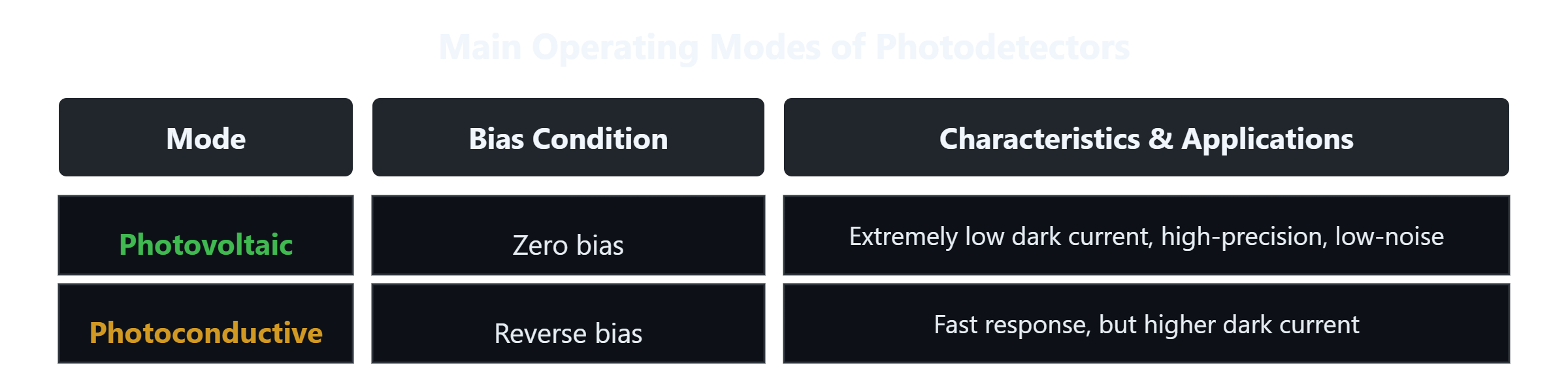
Figure 1: Main operating modes of photodetectors.
1.2 Key Performance Parameters
Responsivity: photocurrent per unit incident optical power, typically 0.5-1.2 A/W.
Bandwidth: 3-dB electrical bandwidth; high-speed detectors require >25 GHz.
Dark current: leakage current with no light, generates noise and reduces sensitivity.
Noise-equivalent power: optical power required to produce a signal equal to the noise power.
Gain: avalanche multiplication factor of APD, typically M = 10-100.
Cutoff wavelength: longest wavelength detectable, determined by the semiconductor bandgap.
II. PIN Photodetector – The Most Basic Product
2.1 Device Structure and Operation
The PIN-PD is the most fundamental and widely used photodetector. Its structure consists of a P-type layer, an intrinsic (I) region, and an N-type layer.
Photons are absorbed in the intrinsic region, generating electron-hole pairs. The reverse bias creates a strong electric field across the I region, causing the photogenerated carriers to drift rapidly and produce a photocurrent.
The thickness of the intrinsic region determines the trade-off between quantum efficiency and response speed.
Transit time is determined by carrier drift velocity and intrinsic region thickness.
RC time constant is determined by junction capacitance and load resistance.
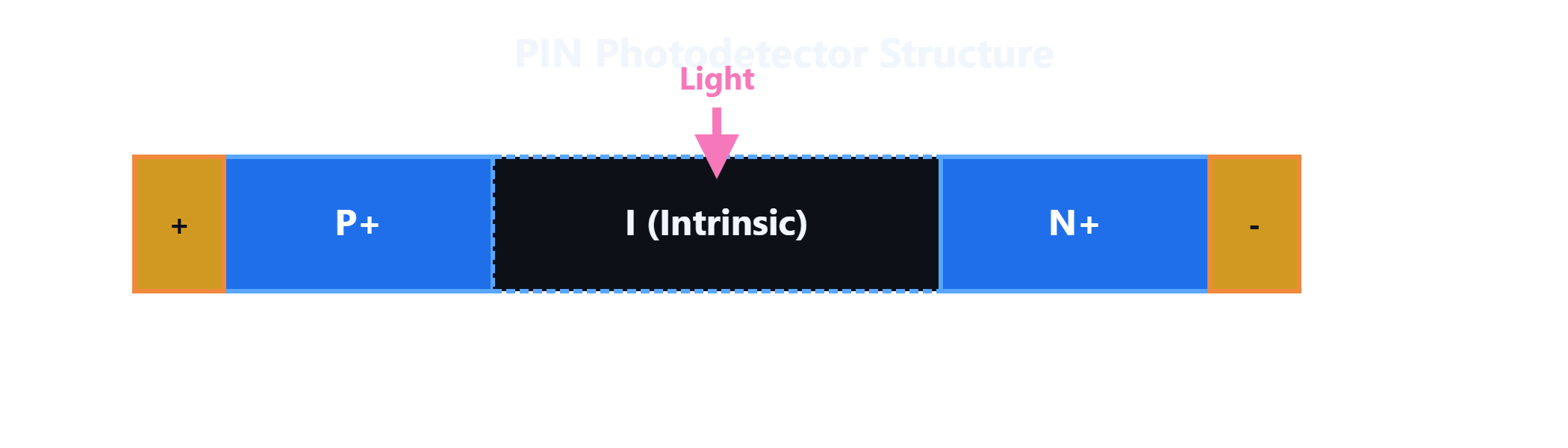
Figure 2: PIN photodetector structure.
2.2 Material Systems and Wavelength Coverage

Figure 3: Common detector materials and their wavelength coverage.
Other commonly used materials include InGaAs (covering 1310/1550 nm, mainstream for communications) and InAs (mid-IR, for gas sensing and thermal imaging). InGaAs PIN-PDs offer high responsivity, low dark current, and excellent reliability, making them the standard choice for 2.5G/10G/25G optical modules.
III. Avalanche Photodetector – High-Sensitivity Product
3.1 Avalanche Multiplication Principle
An APD builds on the PIN-PD by adding a high-field region. When the reverse bias approaches the breakdown voltage, photogenerated carriers gain sufficient kinetic energy in the avalanche region to generate secondary carriers through impact ionization, creating an avalanche multiplication effect and providing internal gain.
Breakdown voltage: bias point where avalanche gain tends to infinity.
Excess noise factor: random nature of the avalanche process causes gain fluctuations, adding noise.
Optimum gain: a gain value that maximizes receiver sensitivity.

Figure 4: APD avalanche multiplication process.
3.2 APD vs. PIN-PD + Electrical Amplifier
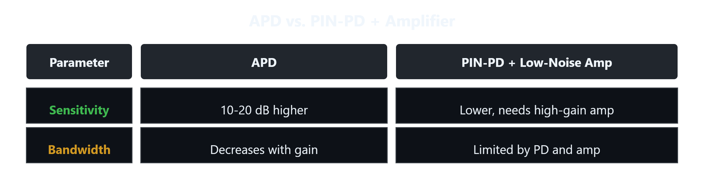
Figure 5: Comparison between APD and PIN-PD + amplifier approach.
APDs require high bias (30-80 V) and their gain is extremely temperature-sensitive, needing temperature compensation. In contrast, PIN-PDs only need -3 to -5 V and simpler circuitry. APDs are advantageous for long-haul (>40 km) or weak-signal detection, while the PIN-PD + transimpedance amplifier (TIA) combination is more common in short-reach high-speed links.
IV. Single-Photon Detectors – Core Products for Quantum Technologies
Why Single-Photon Detection?
In applications such as quantum key distribution (QKD), long-range LiDAR, and quantum computing, optical signals are extremely weak, often at the single-photon level, requiring single-photon detectors.
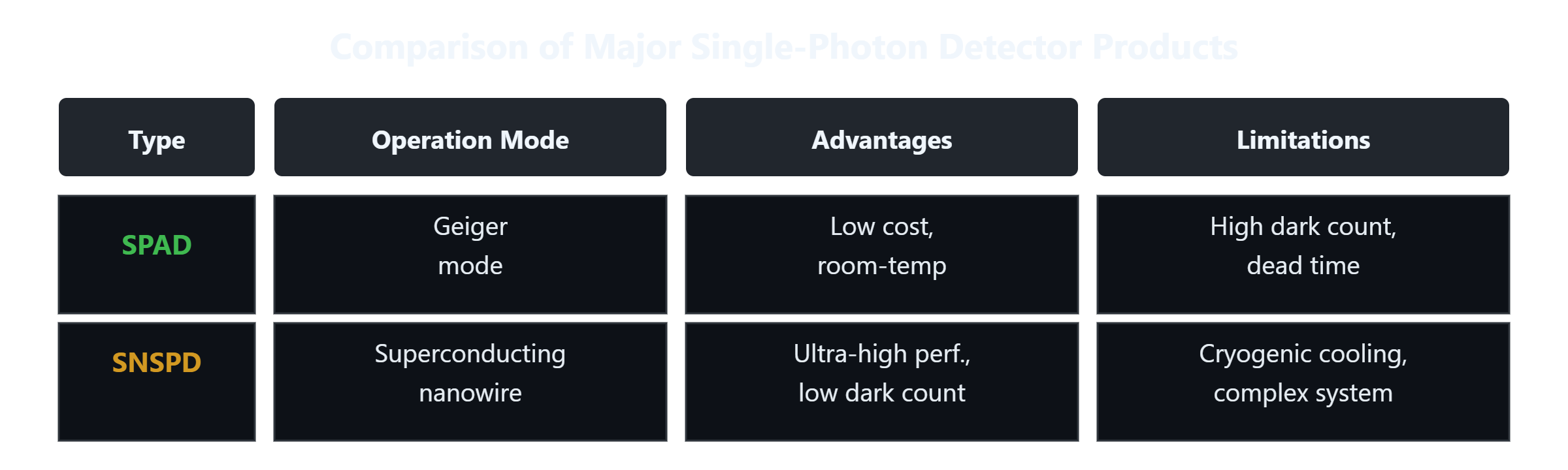
Figure 6: Comparison of major single-photon detector products.
Upconversion single-photon detectors use nonlinear optics to convert infrared photons to visible wavelengths for detection by Si SPADs, avoiding the dark-count issues of infrared SPADs, and have potential in 1.5-μm-band QKD.
V. Photodetector Arrays – From 1D to 2D
1D PD arrays arrange multiple PDs in a line, each with its own electrical contact. They are used for wavelength-division multiplexing (e.g., 4- or 8-channel arrays aligned to different wavelengths) and spectrometers (256- or 512-pixel linear arrays), often packaged in TO-8 or butterfly housings.
2D SPAD arrays are the core of Flash LiDAR, where a pulsed laser illuminates the entire field of view and the array receives echoes from all pixels simultaneously, calculating distance via time-of-flight to achieve 3D imaging without mechanical scanning. Mainstream sizes range from 32×32 to 128×128 pixels, with pitch 20-100 μm; each pixel integrates a SPAD, quenching circuit, and time-to-digital converter (TDC).
VI. Hot Applications and Emerging Technologies
AI Data Center Optical Interconnects
High-speed PDs are the core devices in 400G/800G/1.6T pluggable optical modules. For example, 400G-DR4 uses a 4-channel 100 Gb/s PIN-PD array, 800G-DR8 uses 8-channel 100 Gb/s, and 1.6T-DR8 uses 8-channel 200 Gb/s. The PD arrays are flip-chip bonded to TIA arrays.
In co-packaged optics (CPO), PDs are integrated onto silicon photonic chips (via Ge-Si epitaxy or flip-chipped InGaAs PDs), requiring extremely small footprint, tight alignment tolerance (<±1 μm), and high-temperature operation (85 °C).
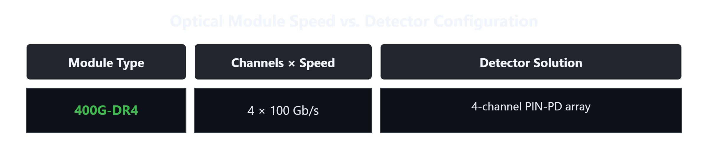
Figure 7: Example of optical module speed and detector configuration.
LiDAR and Autonomous Driving
Time-of-flight (ToF) LiDAR uses APDs (gain M=10-100, bandwidth >100 MHz). Flash LiDAR uses SPAD arrays (single-photon sensitivity). FMCW LiDAR uses high-speed PDs (linear coherent detection). 905 nm Si-SPAD technology is mature and low-cost, making it the current mainstream for Flash LiDAR.

Figure 8: LiDAR detector selection guide.
Quantum Technologies
Quantum key distribution (QKD) commonly uses InGaAs SPADs (gated mode, cost-effective) or SNSPDs (best performance, detection efficiency >50%, dark count<1 kHz, timing jitter
On-Chip Integrated Detectors and Novel Materials
Silicon photonic integrated detectors (Ge-Si, InGaAs-on-Si) are key enablers for CPO and optical computing. Currently, Ge-Si PIN-PDs have achieved bandwidths exceeding 50 GHz, though dark current remains a challenge. 2D material detectors (graphene, MoS₂, black phosphorus) offer atomic-scale thickness, tunable bandgap, and high carrier mobility, promising for flexible optoelectronics, broadband detection (vis-IR), and polarization imaging.
VII. Summary and Product Selection Guide
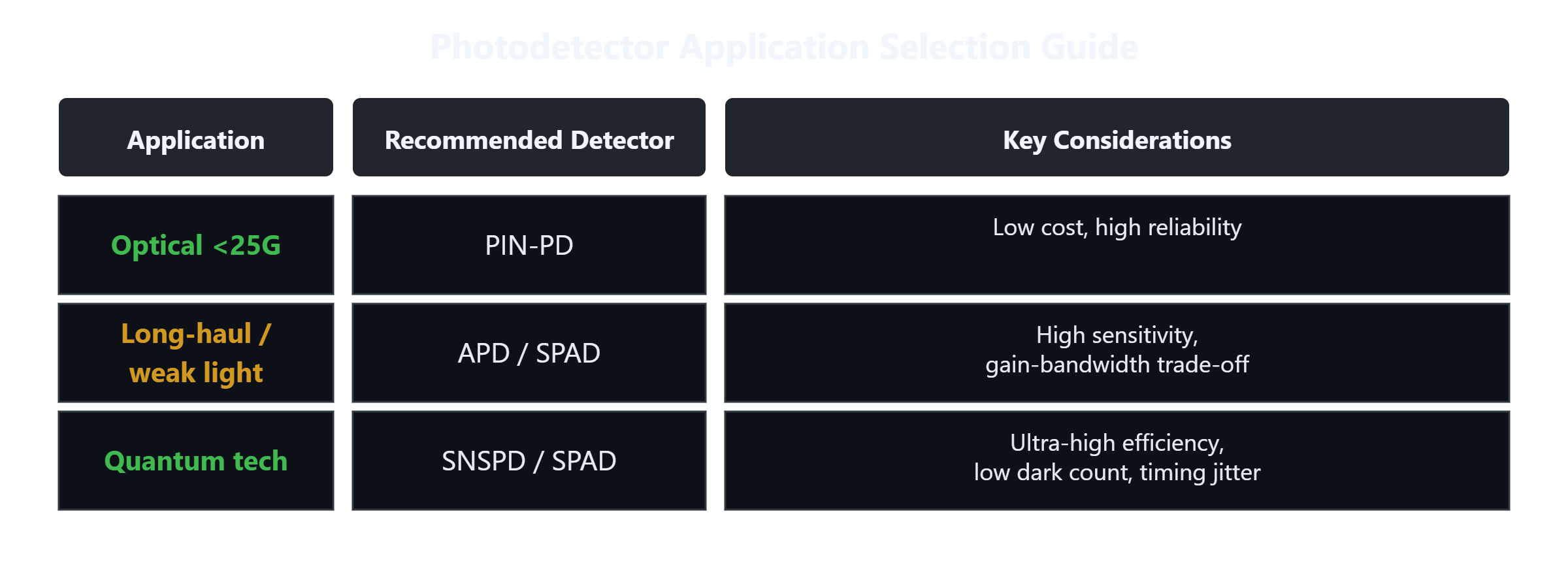
Figure 9: Photodetector application selection guide.
With the rapid development of AI data centers, autonomous driving, and quantum technologies, photodetector products are evolving simultaneously toward miniaturization, on-chip integration, and high-power handling. Mastering the principles and selection methods of photodetectors is a core competence for optoelectronic system design engineers.